VOGONS


First post, by Kahenraz

User metadata
Rank l33t
Rank
l33t

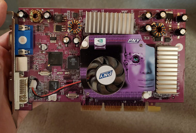
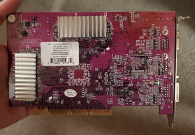
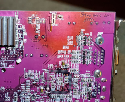
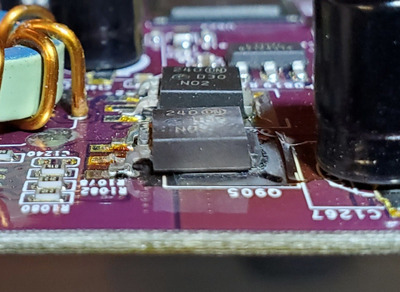
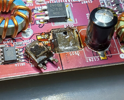
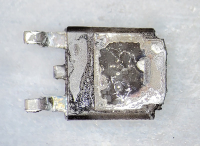
I recently bought this "GeForce4 MX 420" for eBay, which was supposed to be a steal. But it ended up arriving with a burnt up voltage regulator. I recalled seeing some slight discoloration on the rear in the listing photos, but didn't think much of it.

What I think is a voltage regulator is visibly charred, and has even damage damaged the solder mask surrounding it.

I knew from the photos that a lot of the capacitors we're bad, but I was not expecting this. I wonder if the bad capacitors had something to do with the transitor burning up.

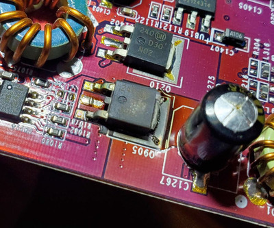
The component is identical to the one directly above it in the photos. Can anyone identify what it is?

Edit:

Check this out. Someone else had this same chip blow up on their GeForce4 Ti:

https://www.electronicspoint.com/forums/threa … ansistor.54344/

20220423_025444_resize_32.jpg
Filename
20220423_025444_resize_32.jpg
File size
218.77 KiB
Views
1029 views
File license
CC-BY-4.0
20220423_025456_resize_96.jpg
Filename
20220423_025456_resize_96.jpg
File size
285.96 KiB
Views
1029 views
File license
CC-BY-4.0
20220423_025516_resize_57.jpg
Filename
20220423_025516_resize_57.jpg
File size
136.13 KiB
Views
1029 views
File license
CC-BY-4.0
20220423_025605_resize_92.jpg
Filename
20220423_025605_resize_92.jpg
File size
141.83 KiB
Views
1029 views
File license
CC-BY-4.0
20220423_032817.jpg
Filename
20220423_032817.jpg
File size
233.08 KiB
Views
1015 views
File license
CC-BY-4.0

Reply 1 of 11, by mkarcher

User metadata
Rank l33t
Rank
l33t

The blown component is an ON Semiconductors NTD30S02 MOSFET. I guess it's possible that the voltage regulator started misbehaving and overheating the FET because the caps are dead, so replacing the FET and the caps is definitely worth a shot. I recommend to check the neighbouring MOSFET for shorts before trying to powering up the card with replaced components.

The MOSFET is a quite generic high power low-RDS-on n-Channel (enhancement mode) MOSFET. I guess the most important specifications are the internal resistance of being definitely below 15 milliohms at 10V control voltage and definitely below 25 milliohms at 4.5V control voltage, with the maximum allowed current of 30 A being common to all FETs which such a low internal resistance. I guess you will have a hard time finding MOSFETs that are unsuitable because they are specified for a voltage lower than the 24V this component is specified for.

Reply 2 of 11, by Kahenraz

User metadata
Rank l33t
Rank
l33t

I removed the MOSFET from this today. It came off "alright", but I had the same problem as with the burned up FET on my Gigabyte GA-P35-DS3P where the component welded itself to the board. I almost got it off safely except for a very small piece that was stuck to the component and tore a hole through the top layer. The solder on the ground pad is also messed up in that I can't get it off the board with solder wick. I think I can still solder a new component onto it, and I'm going to try; I've already ordered a replacement part.

Edit: Looking at it again , I think the reason I can't get the "solder" off is that it's not actually solder but the ground bad off of the bottom of the MOSFET and it has welded to the board; it had delaminated from the component when burning itself up. I know that this wasn't a result of my iron, because I was surprised when it felt like the pad was already loose from the board, after I had lifted the two legs; I could lever it up but it was still stuck at the rear.

20220503_194023.jpg
Filename
20220503_194023.jpg
File size
367.61 KiB
Views
753 views
File license
CC-BY-4.0
Last edited by Kahenraz on 2022-05-04, 17:15. Edited 1 time in total.

Reply 4 of 11, by Kahenraz

User metadata
Rank l33t
Rank
l33t

I really want to do a Twitch or YouTube channel of my repairs, but I don't have the recording equipment for it. If I'm going to be doing all of this repair for anyways as a hobby, I would like to share it with people.

One of the big expenses is that I would need a new trinocular microscope head with a camera mount, lighting, additional cameras... I'm slowly working towards all of this but it isn't something that I can afford to do all at once.

Here is another photo of the ground pad. It's definitely gone and welded itself to the board.

20220504_132428.jpg
Filename
20220504_132428.jpg
File size
210.14 KiB
Views
722 views
File license
CC-BY-4.0

Reply 5 of 11, by TrashPanda

User metadata
Rank l33t
Rank
l33t

Ive seen a few tech tubers actually use old Iphones as a temporary camera setup, sure it isn't super amazing quality but it works quite well, I guess what Im saying here is that your setup doesnt need to be expensive and you could likely get away with far less than you think !

Reply 6 of 11, by Kahenraz

User metadata
Rank l33t
Rank
l33t

At a minimum I would need a new microscope so people can actually see what I'm doing. That's the biggest expense I'm wrestling with, since I already have a microscope, and it wouldn't provide any improvement in my ability to do repairs.

I'll get one eventually. I just can't afford to do it right now.

I have been making smaller purchases periodically as I experiment with other accessories that I want, such as a cell phone arm. I bought one of these squiggly phone arms recently (it arrived yesterday, actually), but I found that it blocked the camera from the rear and was too wobbly and unstable.

s-l1600.jpg
Filename
s-l1600.jpg
File size
75.06 KiB
Views
695 views
File license
Public domain

I've ordered a metal articulating arm next to see if it's any better. If this doesn't work then I'll look at some more expensive options.

s-l1600.jpg
Filename
s-l1600.jpg
File size
103.87 KiB
Views
695 views
File license
Public domain

Reply 9 of 11, by mkarcher

User metadata
Rank l33t
Rank
l33t
Kahenraz wrote on 2022-05-04, 17:16:

Here is another photo of the ground pad. It's definitely gone and welded itself to the board.

I don't think it's actually welded to the PCB, its "just" soldered. MOSFETs die at around 200°C internal temperature, and when they die, they either go short (so the resistance goes down and the heat is generated elsewhere) or in the extreme case, bond wires burn, current stops flowing and again heat generation stops. The back pad of your broken MOSFET is just soldered firmly to the big copper area of the PCB that is very effective at removing the heat you apply with your iron. You likely need to pre-heat the PCB to at least 100°C or use a powerful soldering iron (50W minimum) with the biggest tip you can get to get best heat conduction. With a temperature controlled station, bump it up to 400-450°C temporarily.

Reply 10 of 11, by Kahenraz

User metadata
Rank l33t
Rank
l33t

I have a very powerful Hakko iron and a large tip accessory. I can assure you that it is very unlikely to come off with heat. Even the teeny tiny bit of ground plane that I'd ripped off of the board would not come free of the MOSFET, and had to scraped off with mechanical force.

I performed a similar test on a Gigabyte GA-P35-DS3P with a burned up MOSFET that got so hot that it had carbonized. I had tried inserting a tool underneath to pry it up and inadvertently ripped a hole in the board. At this point I went ahead and levered it up, dangling the MOSFET in the air, still attached to the board by only a thin sliver of ground plane on one of the four sides. I pressed the iron onto the back of it and left it there to see if it would detach, pulling at it with tweezers, but it never did.

I can assure you that heat alone could not have separated it from the board.

Reply 11 of 11, by Kahenraz

User metadata
Rank l33t
Rank
l33t

Following up on this. I still intend to try and fix this. I ordered replacement parts some time ago that are still in the mail.

shipment.png
Filename
shipment.png
File size
29.29 KiB
Views
395 views
File license
CC-BY-4.0