Ohhh...
a very difficult approach that requires deep knowledge. 👍
How do you think is it possible to disconnect the northbridge from motherboard's L2 cache and connect it to L2 on your interposer instead?
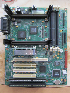
For parts of my investigation, I removed the northbridge from a defective AT motherboard to make some measurements.
The easiest way would be looking into datasheets of chipsets and any L2 cache chip preferable 512 kiB or 1024 kiB. I think manufacturer (EliteMT, UMC or tm) doesn't matter. They all should be pin compatible.
Then you should consider that different chipsets need different tag RAM sizes depending on L2 cache size, e. g. Aladdin V needs 32k8 tag RAM for 1 MiB L2 cache, MVP3 needs 128k8 tag RAM for 2 MiB L2 cache. 32k8 is a 28-pin chip, 128k8 uses 32 pins.
________________________________________________________________________
On my own account:
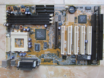
Well, actually I didn't want to buy another Super Socket 7 board. However, one hour before I started my search on ebay some days ago this board was offered there:
An Asus P5A REV. 1.06 with 1 MiB L2 cache for only 35 € + 24 € for shipment!
One should grasp the happiness with hands... 😀