First post, by feipoa

- Rank
- l33t++
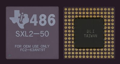
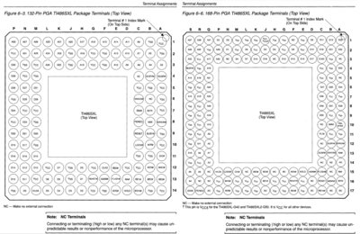
Recently, I created an interposer module to translate the 168 pins (486 socket) of a Texas Instruments TI486SXL2-G66 to that of a 132 pin socket (386). From what I could discern after reading the TI486SXL Reference Guide, found here: https://archive.org/details/bitsavers_tiTI486 … eGuide_19799789 , the TI486SXL2 PGA168 should be the same as the QFP144 and PGA132 variants with minor exceptions. QFP144 and PGA168 have the FLUSH circuits built-in (although you do not have to use them if you don't wire up MEMW#), they have a FLT#, which can be left floating as it contains a built-in pull-up resistor, they run at 3.6 V, and have a few more GND (Vss) and voltage (Vcc) pins.
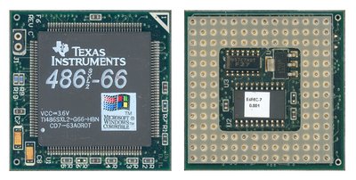
So what would prevent someone from just wiring up the PGA168 pins to the location of the PGA132 pins on an interposer socket and using a voltage regulator module to run the CPU at 3.6 V? The TI486SXL2-66 chips in PGA168 format are readily obtainable new for $15. An upgrade company made such an interposer for the QFP144 TI486SXL2-66 and another user here has tested it. The TI486SXL2-66 (PGA-132)... & repair! and Re: The Systempro; Benchmarking (TI486SXL2-66)
Aside from the IBM BL3 and a Transcomputer module, the TI486SXL2-66 would have been the fastest upgrade for your aging 386. The SXL2 is still architecturally a 386, but with cache and 486 instructions added. Considering how much the SXL2-66 upgrade QFP144 sold for recently, I figured there might be interest in creating an interposer board for the more common TI486SXL2-66 PGA168. I planned to start with a proof of concept prototype, then possibly create a proper PCB if there was sufficient interest.
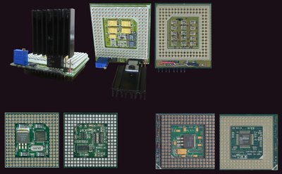
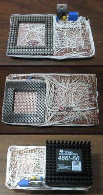
Here is the prototype:
I built the prototype using a snap-able solder boards, a MIC29302WT (LDO = 0.37V @ 3A), 10 uF cermaic input cap, 10 uF tantalum output cap, a resistor, a trimmer, and solid core 28 & 30 AWG wire. I tested several linear and switching voltage regulators before deciding on the MIC29302WT. I finished the prototype after about 10 days of casual soldering.
Unfortunately, I could not get the prototype to work in any of my 386 motherboards. In each motherboard, the TI486SXL2-50 PGA132 CPU worked fine though.
I basically soldered the PGA168 socket directly to the pins of the PGA132 socket using the template found in the TI486SXL reference manual.
The exception is that the Vcc pins on the PGA168 side get wired to the output of the voltage regulator instead of the 5 V line from the PGA132 side (the motherboard). I have the trimmer set such that the voltage to the CPU is 3.60 V. I confirmed this after the prototype was powered on in the motherboard. I have checked each solder connection three times now and also confirmed that none of the wires sorted to any of the other pins, e.g. while soldering some pin, the cladding on an adjacent wire melts and unintentionally caused bare wire to touch. I checked every wire using the beep function on the multimeter to ensure there was no accidental connection somewhere. Perhaps there is still some cross-talk?
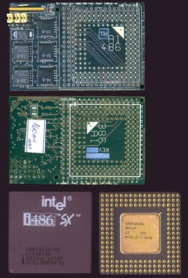
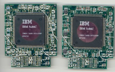
I noticed on the QFP144 upgrade module that there are some extra components, such as additional decoupling capacitors, a NOR gate, and a PAL. Here is what it looks like,
I have come across many 486 upgrade interposer boards which also contain programmeable logic device, such as PALs or GALs, and gate circuits. On many motherboards, these were not required. I believe that they were usually added to increase compatibility with various systems, mostly archaic or non-standard motherboards. Considering that all my 386 motherboards work fine with my 5V PGA132 SXL2 chips, I do not think any special logic would be required on my prototype. Could there be some other difference between the PGA168 and PGA132 SXL2 chips that has eluded me? My gut feeling is that there is something very fundamental I have overlooked. Any ideas? Help!
Concerning the increased number of decoupling capacitors found on the QFP144 upgrade unit; while they may help, I do not believe their absence is causing the no signs of life symptoms. For example, in my experience with these IBM 5x86c-100 chips, the dozen+ decoupling capacitors did not change the stability of the system, not even at 133 MHz. I have two such interposers; on one I removed all the caps, and on the other, I left them on . Both demonstrated equivalent stability in the system I tested them on. While I could add one or two extra decoupling capacitors to the TI486SXL2 prototype, I don't really think it is going to help with the absence of life. The prototype, when installed in the motherboards, does not show any signs of life - that is, the screen never displays anything.
With any luck, I might be able to borrow one of these QFP144 SXL2-66 upgrade kits from a CPU collector and try to determine what they did differently. Obviously the manufactured QFP144 unit is interrupting some pins and taking them to the NOR gate and to the PAL. Unfortunately, I won't know what the PAL is doing, but at least I'd know which pins are interrupted. Perhaps the PGA168 and QFP144 units need some trigger to wake-up, and that is what the PAL is performing? Perhaps the mystery is with FLT#
I have three of these TI486SXL2-66 CPUs and I tried them all, but the result was the same. I also tried setting FLT# to ground at startup and also to set FLT# to GND after power-up, but the result was the same. FLT# is for floating the bus signal. FLT# and MEMW# are the only two pins the QFP144 and PGA168 chips which are not on the PGA132. I do not really understand what FLT# does, but I will copy/paste here what the reference manual says about it.
FLT#
Float (active low). This input forces all bidirectional and output signals to a 3-state condition. Floating the signals allows the microprocessor signals to be driven externally without physically removing the device from the circuit. The microprocessor must be reset following assertion or deassertion of FLT#. This signal may be used in conjunction with an upgrade socket. FLT# is internally connected to a pullup resistor to prevent it from floating active when left unconnected.
MEMW#
Memory Write (active low). This input is used in the cache interface logic which flushes the cache in systems that hold the CPU during DMA and MASTER cycles.
MEMW# is the pin which leads to the hardware flush circuit (NAND gate and an inverter) inside the PGA168 and QFP144 chips. You connect MEMW# from the motherboard's ISA bus to MEMW# on the CPU. This is why the prototype has a single header. Anyway, the motherboard I'm testing already has this circuit built in, so this pin is not needed. The motherboard's circuit drives FLUSH# directly, which performs the same function. Connecting or not connecting this should not prevent the motherboard from powering up.
I tested the prototype using 50, 66, and an 80 MHz oscillators. If there is cross-talk issues, I figured running the CPU at 25 MHz would have at least showed signs of life; it did not. I tested the motherboard with MR BIOS and the original AMI BIOS. I tested with the FPU installed, removed, and with the co-processor jumper set to off. Still no signs of life.
The next logical step would be to test the TI486SXL2-66 in a 486 motherboard. Problem is that I haven't seen and do not have any boards which have jumper settings for this CPU. Although the TI486SXL2-66 has a nearly identical pinout to the Intel 486SX, a few modifications must be made to a non-supporting 486 board to use this CPU. The TI486SXL reference manual goes through the few design considerations in Appendix D for motherboards wanting support for the TI486SXL. There is about a four jumper difference, which would be fairly easy to implement on your 486 board if one doesn't mind modifying their boards. This would just verify that the TI486SXL2-66 chips I have are indeed functional. It does seem unlikely that three NOS chips would be bad though.
I also tried using the Transcomputer 486HPi upgrade module with the TI486SXL2-66 installed. I set the Transcomputer module up for 486SX pinout, but I did not see any signs of life when powering on the system. An Intel 486SX CPU, on the otherhand, worked just fine on the same 386 motherboard. This confirms that there are differences which need to be considered with getting a 486SXL2-66 working on a 486 motherboard. I tried the TI486SXL2-66 in the Transcomputer at 5 V and at 3.6 V (by using a variable voltage VRM on top of the Transcomputer).
EDIT: Here are two URL's to the TI486SXL and TI486SXLC reference book
https://ia803003.us.archive.org/35/items/bits … rence_Guide.pdf
http://www.bitsavers.org/components/ti/TI486/ … rence_Guide.pdf
Plan your life wisely, you'll be dead before you know it.