VOGONS


Reply 80 of 1184, by cb88

User metadata
Rank Newbie
Rank
Newbie

KiCad 4.0.7 is the old stable yes... But 5.0 will be the new stable in a month or so and has huge improvements....the accelerated modes are actually usable not so it should actually run faster than 4.0.7..... and with exception of the ratracer it does work on xpsp3

Also have you got an eBay link to that I don't see them at all. Perhaps they only ship to canada so I can't see it from the USA? Actually found it searching Ebay.ca... not sure why it isn't showing up in the USA as it is shipped from the USA.

Reply 81 of 1184, by feipoa

User metadata
Rank l33t++
Rank
l33t++

Found 'em 'eh? Pretty good deal if you live in the USA.

I was thinking that a working interposer for the SXL2 will make my rare Evergreen SXL2-66 on QFP144 to PGA132 adapter less valuable, but its far better to open this upgrade up to everyone.

Do you have a direct link to the 32-bit version of KiCad 5.0 for XP?

Plan your life wisely, you'll be dead before you know it.

Reply 82 of 1184, by cb88

User metadata
Rank Newbie
Rank
Newbie
feipoa wrote:

Found 'em 'eh? Pretty good deal if you live in the USA.

I was thinking that a working interposer for the SXL2 will make my rare Evergreen SXL2-66 on QFP144 to PGA132 adapter less valuable, but its far better to open this upgrade up to everyone.

Do you have a direct link to the 32-bit version of KiCad 5.0 for XP?

Just grab the latest i686 file from here... just beware its an 850MB download.
http://downloads.kicad-pcb.org/windows/nightly/

Reply 83 of 1184, by feipoa

User metadata
Rank l33t++
Rank
l33t++

There's a lot of files in there. Is this the one you are using?:

kicad-r10615.1a2291879-i686.exe 14-Jul-2018 17:04 859463086

Plan your life wisely, you'll be dead before you know it.

Reply 84 of 1184, by cb88

User metadata
Rank Newbie
Rank
Newbie

It doesn't matter all of them should be recent enough... KiCad has been in feature freeze for quite awhile not they are just working out any last minor bugs. Just use the one with the latest date.

Reply 86 of 1184, by cb88

User metadata
Rank Newbie
Rank
Newbie

Just uploading so you can sanity check my schematic, the one on one on the left I should have correct I used the pin mapping from 6-5 here http://bitsavers.trailing-edge.com/components … rence_Guide.pdf

I'll probably finish mapping the one on the left (the 168pin) Wednesay or later this week referencing this. https://ia601003.us.archive.org/21/items/bits … rence_Guide.pdf

Note the 132pin pinout is missing MEMW# and FLT# and the A10 reserved pin.

The one on the left I will need to remap the pins in the symbol still since it doesn't match the 168pin pinout yet.

I also took the liberty to pretty up the symbol and make it more descriptive of the pins enjoy!

Attachments

  • Filename
    CPUInterposer386-486.pdf
    File size
    115.14 KiB
    Downloads
    79 downloads
    File comment
    Schematic
    File license
    Fair use/fair dealing exception

Reply 87 of 1184, by feipoa

User metadata
Rank l33t++
Rank
l33t++

You definitely want to use the SXL2 spec sheet and not the DLC one. There are a few pin differences. There is a complete mapping table on page 4-4 thru 4-12, which I assume you've found by now. You'll want to check my notes above.. MEMW# should go to a header on the PCB. FLT# can be left floating. Vcc5 should be left at 5 V. I have no idea what A10 is for. There should also be a header for 5 V on the PCB to run a 5 V fan.

Plan your life wisely, you'll be dead before you know it.

Reply 88 of 1184, by cb88

User metadata
Rank Newbie
Rank
Newbie

Yeah I'll double check the 132pin symbol later. I was just updating the 168pin symbol to have the few extra pins it is suppose to have. + extra power/gnd also, Wired the 132pin to 5v and 168pin to Vcc since that'll be from a regulator.

I figured that was the case with FLT# the SXL datasheet kinda indicates that, but wasn't sure about MEMW#.

I had forgotten about Vcc5 should have known there'd be one of those... but I'm kinda doing this quick anyway in my spare time. Worst case you at least get a premapped schematic aka the not fun part!

Attachments

  • Filename
    CPUInterposer386-486.pdf
    File size
    114.66 KiB
    Downloads
    62 downloads
    File comment
    Update SXL symbol, minor rewiring, add fan header
    File license
    Fair use/fair dealing exception

Reply 89 of 1184, by cb88

User metadata
Rank Newbie
Rank
Newbie

All the Pins ar mapped, added the regulator (probably going to switch it and the header to surface mount parts to save room.
https://drive.google.com/file/d/1f7RzduwZmOqD … iew?usp=sharing

Was just playing around with routing some of it... it's a bit messy and I haven't routed something like this before so a bit of a learning curve.

Attachments

  • Filename
    CPUInterposer386-486.pdf
    File size
    118 KiB
    Downloads
    61 downloads
    File comment
    Current schematic that that matches this zip file
    File license
    Fair use/fair dealing exception
  • interposer-pcb.PNG
    Filename
    interposer-pcb.PNG
    File size
    132.27 KiB
    Views
    1016 views
    File license
    Fair use/fair dealing exception

Reply 91 of 1184, by feipoa

User metadata
Rank l33t++
Rank
l33t++

There is no urgency here.

To reduce the footprint, I suppose we can eliminate the 5V/GND header. The user can always use the molex for their fan. It would be nice to keep the foot print as small as possible because you don't know what might be in the way on these 386 boards. Sometimes jumper headers are placed close to the PGA132 socket.

As noted earlier, I suggest using SMD for the VRM and place it under the PGA168 CPU. Also use a mini dip switch for 6 values of VRM voltage. Do you need me to lookup a mini DIP switch part number?

Since I think we should remove that orange line in the above wiring schematic, the main issue bothering me is where to place the MEMW# header. I was thinking you might be able to use a 90 degree bent single-pin header and put it on the underside of the PCB. Where? On the part that is nearest to the edge, past where the the PGA132 pins are. Perhaps diagonally between the PGA168 pins, just as the PGA132 pins are in between the PGA168 pins. What do you think?

Plan your life wisely, you'll be dead before you know it.

Reply 92 of 1184, by cb88

User metadata
Rank Newbie
Rank
Newbie
feipoa wrote:

There is no urgency here.

Huh? I tend to procrastinate personal projects a lot so... urgency would at best just motivate met a bit to do it 🤣. It's not like I am rushing or anything... making progress is a motivator in itself of course.

VRM under the chip is probably a non starter for OC for normal clocks it might be fine... you'd have a chip dissipating a over watt or two *under* your CPU this alone would probably reduce potential for OC. A not insignificant amount of heat actually dissipates into the PCB under normal conditions... but the interposer itself is already reducing that. I don't mind making a version like that but I am more inclined to stick the VRM off the side somehow or make the board bigger.

The 5V header will be surface mount .. making in a non issue it's still a cheap part and won't be an issue on the bottom side there is plenty of room to solder it. Perhaps make it a 3pin and route the MEMW there... just for simplicity Labeled of course on the silkscreen.

I already have a mini switch in mind I've used them before quite small... https://www.digikey.com/product-detail/en/nid … 042-2-ND/948353

@luckybob care to explain that comment 🤣 I'm actually not that great at reading facial expressions... ?

Also I am inclined to forgo attempting to dogbone the pads and just doing via-in-pad since it's mostly going to be hand assembled , solder pasted and probably reflowed in an oven anyway thoughts? I might give some of this low temp stuff a try... https://www.amazon.com/Clean-Temperature-Sold … ds=solder+paste

Also what orange wire? This is a 4 layer stackup... the orange wire I guess you are referring to is an inner layer I am probably going to try routing all the signals on the inner layers next time. One problem is that is 0.5oz copper there maybe not a big deal though. Outer layers are 1oz or greater depending on how you order it.

Reply 93 of 1184, by feipoa

User metadata
Rank l33t++
Rank
l33t++

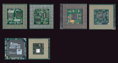
I am not too concerned about the VRM being under the CPU. Here are some examples of popular upgrade companies doing it. One one such upgrade interposer, it ran the Cyrix 5x86-133 "chili pepper". From the name, you get the idea that it ran hot. I've attached one such interposer which is of the same chip we are using, the 486SXL2-66 at 3.6 V. The VRM is under the whole interposer. This configuration ran fine for me at 3.6 V and 80 MHz. I suspect 3.6 V and 80 MHz will be the norm for this interposer board. I suspect most people would prefer the clean look and reduced real-estate of this design. However, I do also like the idea of two models. In the second model "B", how about keeping the trimmer, through hole VRM, and 3-pin header?

Interposers_with_VRM.jpg
Filename
Interposers_with_VRM.jpg
File size
980.03 KiB
Views
991 views
File license
Fair use/fair dealing exception

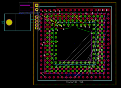
In my previous message, I said "orange line", not "orange wire". There is only one orange square line in layout schematic you provided. My hope was that for model "A", the PCB real-estate would stop at the white square line, thus eliminating the extra area provided by the orange square line. If you are not familiar with using upgrade adapters on 386 boards, you may not understand why I am trying to keep the surface area of the PCB the size of the PGA168 CPU. What often happens when using these larger bulky interposer upgrades, the user must stack up male-to-female PGA168 sockets underneith to lift the PCB over motherboard components. I'm hoping to avoid this entirely. For model "A", refer to the interposer example by Trinity Works Inc (provided). For model "B", I suggest making it like the other interposer example, the one with "By D.M." printed on the PCB.

That mini DIP switch is similar to the one I had in mind. Do you want the 8 positions? Also, the part number you listed on digikey is asking for an order quantity of 2,000.

For 6 switches, you may consider, https://www.digikey.com/product-detail/en/nid … 10-6-ND/1853740

Or for 8 switches, you may consider, https://www.digikey.com/product-detail/en/nid … 012-1-ND/948432

These have single unit order availabilities. They are 6 V, 100 mA.

Looks like we can get lower profile (1.55 mm vs. 2.5 mm) with 24 V, 25 mA. I don't expect the current to get anywhere near 25 mA.
6 switches, https://www.digikey.com/product-detail/en/omr … 1116-ND/1811597
8 switches, https://www.digikey.com/product-detail/en/omr … 1118-ND/1811600

I somewhat prefer the dog bone approach because it looks a lot more period correct for 1993-1994 interposers. But if it won't work, then let it go. Any risk with the via-in-hole approach? Is it less reliable for users using a metal-pointed solder iron? I suspect that is what most people would use.

I personally haven't used solder paste before. I suspect this also takes some trial and error - e.g. if you don't use enough, you don't get a reliable joint. Don't heat long enough, don't get a reliable joint. Heat too long, etc... What are your thoughts here? It seems unlikely to me that the user group here will want to experiment with this. I assume the assembler is responsible for putting the paste on. What if too much is put and it bridges junctions?

Plan your life wisely, you'll be dead before you know it.

Reply 94 of 1184, by luckybob

User metadata
Rank l33t
Rank
l33t

Actually I would look into a selectable power delivery setup. Something similar to what power leap did with Socket 7 cpus.

A 100mhz 486 draws about 8W right? At most a 100% overclock so 16W and a bit of overhead gives 20W a nice round number. I would make it adjustable from 3v to 5v.

I'd drop in something like this: https://www.mouser.com/ProductDetail/GE ... sGeYjCg%3d add a few resistors selectable by switch (or adjustable pot) and you can get any voltage you want. It even will take 12v power so you can just connect a power lead directly from the motherboard, just like the powerleap socket 7 one.

This would have the advantage of taking the motherboard power delivery out of the equation. There are more robust models out there with tighter tolerances but the price goes up real quick for these things.

I've used solder paste and it is fine for SMD parts. You get a stainless steel template of the board, apply the paste, scrape off excess, remove template, place the smd parts and drop into an easy bake oven. It is standard smt soldering. Also, I request the use of MELF resistors. ^.^

I'm going to play with this a bit.

It is a mistake to think you can solve any major problems just with potatoes.

Reply 95 of 1184, by feipoa

User metadata
Rank l33t++
Rank
l33t++

luckybob, do you know what the voltage drop-out is on that item? Normally regulating from a 5 V supply down to, say, 4.5 V will require a very low drop-out condition. Taking 12 V power from the molex is not very elegant.

In all practicality, most 386 boards will not work with a 100 MHz oscillator. If they do, the L2 cache is unlikely to work. I also doubt that the CPU itself will work at 100 MHz. This is why I am pushing for a sleeker design. I do like the option for two designs, 'A' and 'B'. The most likely condition is 80 MHz at 3.6 V. I'd certainly like to find some 88 oscillators in the SIP/DIP-14(?) package. 88 MHz may be a more realistic end point.

Plan your life wisely, you'll be dead before you know it.

Reply 96 of 1184, by luckybob

User metadata
Rank l33t
Rank
l33t

Well according to the PDF spec sheet, they have characterized the converter with 1.5V overhead minimum. So if you wanted 5v out they tested it with 6.5V input. So I would assume 3.5V would be the realistic maximum with 5v. I don't see an issue using the 12v directly from the PSU. @5v the efficency is >90% which is damn good. Obviously I was just using this as an example of what I had in mind with the form factor. There are 10's of thousands of dc/dc converters for selection on mouser, I just picked one that looked the way I had it in my mind that would "work".

It is a mistake to think you can solve any major problems just with potatoes.

Reply 97 of 1184, by luckybob

User metadata
Rank l33t
Rank
l33t

Also as for the power requirements, I just took what I felt would be a worst case scenario approach. Design for the worst case, then you can scale back if it is too much. For a power supply they tend to be most efficient in the middle 1/3 region. Obviously this is not that important to be so efficient, but it is a good practice imho.

It is a mistake to think you can solve any major problems just with potatoes.

Reply 98 of 1184, by luckybob

User metadata
Rank l33t
Rank
l33t

There is also the cheap chinese route: https://www.ebay.com/itm/DC-Step-Down-Adjusta … 353.m1438.l2649 I use something similar in my storage server. I have 12 of these things powering 24 hard drives. dropping 12v to 5v. The one I linked is adjustable. Those little 8-pin chips are amazing. spec sheet: https://www.monolithicpower.com/pub/media/doc … MP1584_r1.0.pdf

Granted the form factor is an issue, but the circuit would be simple enough to copy onto the adapter.

It is a mistake to think you can solve any major problems just with potatoes.

Reply 99 of 1184, by cb88

User metadata
Rank Newbie
Rank
Newbie
luckybob wrote:

There is also the cheap chinese route: https://www.ebay.com/itm/DC-Step-Down-Adjusta … 353.m1438.l2649 I use something similar in my storage server. I have 12 of these things powering 24 hard drives. dropping 12v to 5v. The one I linked is adjustable. Those little 8-pin chips are amazing. spec sheet: https://www.monolithicpower.com/pub/media/doc … MP1584_r1.0.pdf

Granted the form factor is an issue, but the circuit would be simple enough to copy onto the adapter.

My actual comment got lost earlier sorry editing to fix it.

I may just add a header so you can select the input of the on board LDO... so you can get the benefit of using a switching PSU like that for where the on board LDO needs more voltage.