So it seems that the GAL has a lot of responsibilities in this design. If you think it will be difficult to understand every GAL function maybe cloning the code is the only way. Also it seems that only a few traces are left to be detected?
If you think it will be difficult to understand every GAL function maybe cloning the code is the only way. Also it seems that only a few traces are left to be detected?
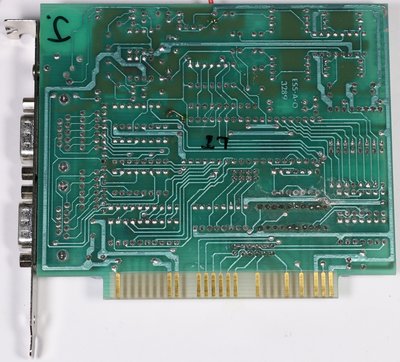
There are many traces still hidden. Especially in the analog section. But as about GAL funtions - I think I could figure out address decoding and read/write/latch control logic. But I need to know address map for this card.
I thought Yvan256 had a programming manual and was going to share it here, but I didn't see it.
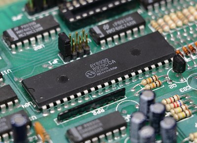
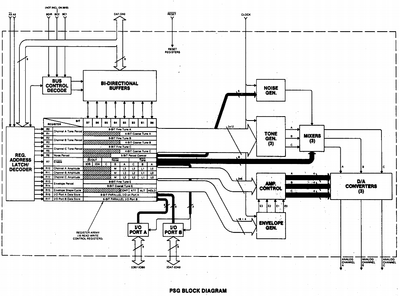
In the meantime I'm trying to figure out main differences between AY-3-8910/AY8930/YM2149 and SAA1099 (CMS) and SN76489AN (Tandy/PCjr). On paper all those seem to be square waveform/noise generators with 3 voices... 😅
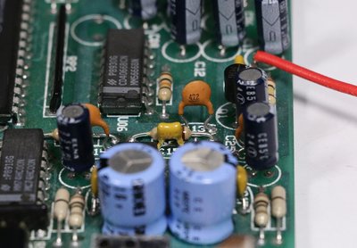
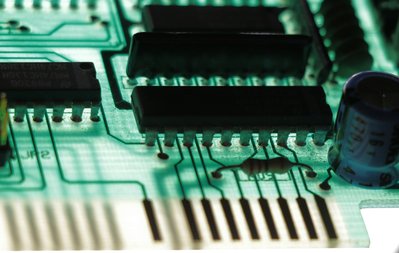
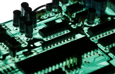
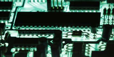
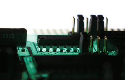
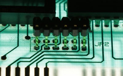
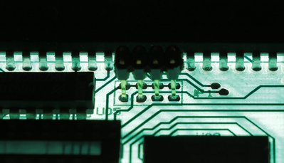
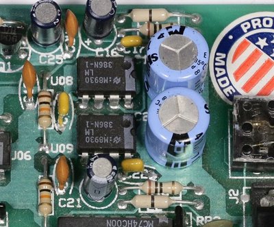
Instead of sleeping before a work day, I've spent half of the night looking under ICs on the board with strong backlight. 😒
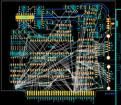
The result is: I've traced out 99.9% traces under logic ICs (while correcting some errors I've made before) and most of the traces on the analog part of the board.
The question is now: how replica should look like?
I'll try to make a small "block" from it for the FMonster, so completely re-routed compact SMD layout is out of the question, it will be done.
But for the "original replica" what should be done?
1) Component placement and routing:
a) should be left as close to original as possible (even if it degrades output quality and looks bad);
b) can be re-done in some places to get some improvements;
c) should be fully made from scratch (as an example: Malinov's OPL2 board vs. AdLib).
2) Components on the board:
a) should stay as they were: in same packages, all through-hole;
b) should be replaced with compact SMD analogs where possible.
3) Joystick ports:
a) will be implemented as on the original;
b) will be implemented as standard 15-pin PC joystick port;
c) will be removed.
Please give some answers like "1.a, 2.b, ...".
Keep in mind, that there can be more than one variant made. So, you can give a series of answers for multiple boards in order of decreasing importance.
I will go with: "1.b, 2.a, 3.c" and "1.c, 2.b, 3.c" (and a variant of the latter for the FMonster). But that's just me.
1.x) Combination of B + C - try to keep the general component placement, but place them as tight as possible (<3 small, well packed PCBs) - if possible replace the GAL with standard 74-family logic and the resistor DAC with it's uncommon values for a real R2R ladder/DAC-chip.
2.a) I prefer SMD, but since I guess going full SMD isn't possible and it's intended as a kit/diy project going with through hole will be the least hassle.
3.a) Definitely A - the 9 pin Atari/Kempston style joystick ports are one of the most prominent features of the card.
Combination of B + C - try to keep the general component placement, but place them as tight as possible (<3 small, well packed PCBs)
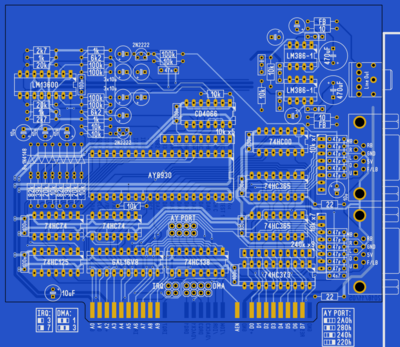
For the moment I'm going for 1.c+2.a. It is a pain to look at original routing, it is very confusing, cumbersome, it has many errors. I don't want to touch it. I'll make my own. But trying to preserve looks of the original board in the process.
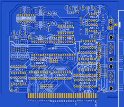
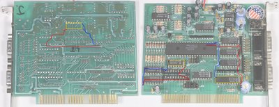
Here is crude copy of original routing:
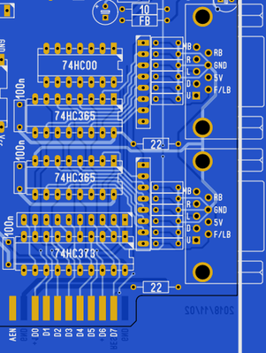
Some improvements in that spot already:
- connections of 74HC365 are mirrored between joystick ports (originally those are very different)
- significantly less loop area of power rails of each IC
- added fusable resistor to joystick power rail (external short protection)
- added bypass capacitors for logic ICs
shock__ wrote:
if possible replace the GAL with standard 74-family logic
That is out of the question for the moment. You have to ask moturimi1 about what is being done with GAL chip now. Without user's manual I can not tell anything about port offsets for each components and modes of operation.
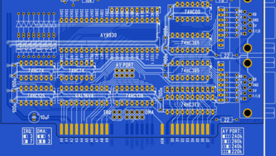
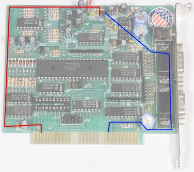
But, with fully restored connections, I have now information about possible base addresses (that are decoded by 74HC138) and those are somewhat problematic. 😐
Rightmost position (marked "1") sets base address as 0x220, that at least intersects with OPL2, OPL3 and CMS addresses.
Next position ("2") sets base address as 0x240, "3" sets 0x280 and "4" (leftmost) sets 0x2A0. And those values can conflict with CMS or SSI one way or another. So carefull port setting will be required.
Note: 74HC138 itself decodes space up to +0x020 from the base address (0x240...0x25F if "0x240" is selected). So, anything inside that span is decoded via GAL.
shock__ wrote:
resistor DAC with it's uncommon values for a real R2R ladder/DAC-chip
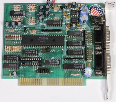
There are, actually, TWO different DACs on this board. 😲
One is on the left side (8 resistors and diods), it sets two 4-bit values for LM13600 amplifier on inputs called "AMP BIAS INPUT". It is controlled via I/O port A of AY IC. Output of that amplifier is going straight to the output stage of the card. Positive inputs of LM13600 are connected via some resistor networks and switches to Channel A and Channel B outputs of AY. I presume that this "DAC" is used as 4-bit stereo volume control.
Second is in the bottom right corner: 74HC373 with resistor network. 😲 It is controlled by one logic line from GALpin 19, enabling this signals allows anything from ISA data bus to be passed and latched for resistor network. Common pin of that resistor network is connected to ground, first resistor is the output and goes into analog part of the board and probably is mixed via resistor networks into LM13600 inputs. All other resistors are connected (virtually, via 74HC373 latch) to D7...D0 if ISA data bus in sequence. So... probably it is some kind of PCM playback DAC. Probably this is the thing that requires DMA via GAL. 😕
And the last bit about GAL pinout.
Previous research was done here, make sure you've read it.
Now some updates on that. Pin 6 (input only for GAL) is connected to I/O port B bit 5 of the AY and resistors between AY and analog switch CD4066. So I presume that pin of I/O port B is used as output and it affects GAL in some way. 😕 Pins 15, 16 are connected to BDIR and BC1 inputs respectively of the AY chip, controlling its behavior. So those pins of the GAL are outputs. Pin 17 is connected to /OE1 and /OE2 inputs of top 74HC365. This pin is output on the GAL. It allows status of all 6 buttons of the top joystick (marked as "1" on the bracket) to be put straight to ISA data bus at D0...D5. Pin 18 is connected to /OE1 and /OE2 inputs of bottom 74HC365. This pin is output on the GAL. It does all the same things, but for joystick "2" (bottom one). Pin 19 is connected to LE input of the 74HC373. This pin is output on the GAL. As was described above, it allows data from ISA data bus go to "resistor network DAC" and, probably, to PCM playback that way.
So, total map of pins 12...19 (that could be configured as inputs or as outputs on the GAL) is: OOIOOOOO.
At the moment, almost all connections in the digital part of the board are done. It became a little smaller, than original and ICs are aligned with each other where possible.
Now it's time to wrap my mind about LM13600 function in this board and proceed with analog part of the board.
Also, I have a question for everyone here.
Do we really need LM386 amplifiers? Those are used to drive low power passive speakers, those are not needed for line output.
I will go with: "1.b, 2.a, 3.c" and "1.c, 2.b, 3.c" (and a variant of the latter for the FMonster). But that's just me.
I agree with your choices.
About output: if a modern replacement is more suitable than using those old LM386 amps i am for it, i trust that you will make a good choice.
Your work is impressive Fagear, thank you so much for your effort, soon we will have a CSM replica!
About thread: i launched it some 4+ years ago but i cannot move it, so maybe a moderator can do that for us, i agree this thread belongs in the Sound section.
But, with fully restored connections, I have now information about possible base addresses (that are decoded by 74HC138) and those are somewhat problematic. 😐
Rightmost position (marked "1") sets base address as 0x220, that at least intersects with OPL2, OPL3 and CMS addresses.
Next position ("2") sets base address as 0x240, "3" sets 0x280 and "4" (leftmost) sets 0x2A0. And those values can conflict with CMS or SSI one way or another. So carefull port setting will be required.
I don't think you need to worry about that too much.
If you look at the Tandy clone card, the original C0-address was problematic. We solved that by introducing new addresses and just patching software.
So if you can't make all sound chips work together on their 'default' addresses, you could just pick a new address, and we can patch the games. There's only a handful of games that support the card anyway.
Mind you, an alternative would be some kind of switching logic. Technically there is absolutely no problem if two or more chips share the same base address, IRQ or DMA channels, as long as they don't use them at the same time.
This would be most interesting if you wouldn't have to open the case to configure it. So if there were some convenient jumpers on the card, they could be connected to a few switches, that can be installed on a backplate or a drive bay.
I used to have a switch connected to my SB Pro 2 and my GUS, installed in a drive bay at the front of my PC. Flick the switch one way, and the SB was 220h, GUS was 240h. Flick it the other way, and the SB was 240h, the GUS was 220h (had to re-run the GUS-init program and update the BLASTER and GUS env vars, but that was easy enough from a bat file).
I probably can't contribute to this in any way, but I'd really like to point out that I'm really impressed with your work and that I really appreciate it. It's projects like this and people like you that keep the retro community alive. Good luck and keep up the good work! 😊
Mimi: AMD K6-2/266, S3 Trio64, Diamond Monster 3D II, Sound Blaster CT2800, 32MB RAM Satellite 220CS: Pentium 133, SVGA DSTN, Sound Blaster Pro, 64MB RAM Contura 420CX: 486DX4 75, VGA TFT, Roland Serial MIDI, 16MB RAM
Do we really need LM386 amplifiers? Those are used to drive low power passive speakers, those are not needed for line output.
LM386 has pretty mediocre specs. Maybe just replace it with good dual OpAmp (4558/5532/2134, whatever) for line out and that's all? 😕
I'm not especially knowledgeable about such topics, but I'm pretty sure the sound chip (AY8930) and DAC on this card technically only support monophonic output, with no way for software to do arbitrary stereo panning. (Actually the AY8930 has individual outputs for each of its three voices, but I assume the original card mixes them into one and doesn't pan them around like some machines do with the AY-3-8910). If so, perhaps it's fine to go with a monophonic DAC instead, assuming such a thing exists and if it would further decrease the complexity of the PCB design/routing.
...I'm pretty sure the sound chip (AY8930) and DAC on this card technically only support monophonic output, with no way for software to do arbitrary stereo panning. (Actually the AY8930 has individual outputs for each of its three voices, but I assume the original card mixes them into one and doesn't pan them around like some machines do with the AY-3-8910). If so, perhaps it's fine to go with a monophonic DAC instead, assuming such a thing exists and if it would further decrease the complexity of the PCB design/routing.
You are not 100% correct. AY IC has three independent analog outputs: Channel A, Channel B and Channel C.
Those are equal.
In some Spectrum computers those outputs were just downmixed to mono, but in others it was connected in stereo configuration.
One channel was connected to left output, another channel was connected to right output and third channel was connected to both outputs. Order (ABC) of channels was different from computer to computer, so you often could select in a software the order of channels on your exact variant.
DAC is another story... more on that later.
I've digged deeper into all of outputs and mixing of this board... It is a mess. I don't know what were developers of this board thinking. 😳
Analog channels A and B are indeed connected to different output channels of the soundcard. Thus you have two LM386 amplifiers onboard - it is in stereo. Channel C could be connected to both output channels. Could be, but it is not always connected. That's where weirdness starts. 😖
Analog output of Channel C from AY takes two paths.
One way is to the input of CD4066 analog switch, that is controlled from pin 7 on I/O port B of the same AY chip. Strange, but whatever. If switch is enabled then output gets mixed into both output channels via resistor mixer at same volume as Channel A and Channel B.
But there is the second way. Through the cascade on one NPN transistor it goes into... counting input of the 74HC74! 😲 Output of that D-trigger goes into 74HC125 buffer, then, if HC125 has "enable" signal, its output goes... to ISA DRQ line (DMA request)! Weirdness does not stop there. That "enable" signal for HC125 comes from pin 7 on I/O port B of AY chip, the same pin that controls switching of Channel C to analog output mixer! 🙄 A cherry on top is circuit that resets output of 74HC74 D-trigger: it is a series of NAND gates (74HC00) that sums inputs ISA_RESET and ISA_DACK (DMA acknoledgement).
So... Analog Channel C of the AY can work in two modes:
1) as normal analog output mixed as mono into output
2) as... (timed?) driver for requesting DMA from ISA bus?.. 😳
That's not everything strange in this board.
IRQ signal for ISA bus is also controlled by AY chip! The signal itself starts at GAL, that can drive Count input and Clear input of another D-trigger in 74HC74. Output of that trigger goes into another buffer in 74HC125, but before it can become ISA_IRQ signal, it must be allowed by... pin 6 on I/O port B of the AY. What the ...
And this is not finished just yet. There is one more analog switch that is controlled... You guessed it, by pin 4 on I/O port B of the AY chip. What it does? It just shunts outputs of Channel A and Channel B together (to get two channels in mono)! Screw resistor mixing and everything, just short those outputs of AY together! Why do I think that shorting two pretty low impedance outputs is a bad idea? 🙄
Well, enough of AY. Ok, it has three weirdly mixed outputs that somehow go into stereo output.
But there is one more sound source on that board, that I've mentioned earlier. That is the DAC that is formed by 74HC373 and resistor network. It is indeed, as SW-SSG was mentioning, mono. And signal from that gets buffered through emitter follower on another NPN transistor and then is mixed into both analog outputs (as mono).
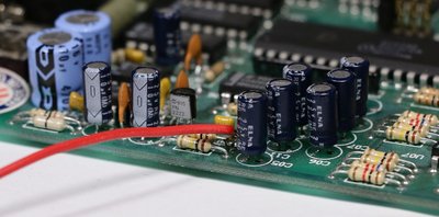
There is another... well, not weirdness, but just plain error of developers of this card. 😵 Power layout. It gets power from +5V ("digital") rail, trace for it goes through the top of the board to the very left (if we look at components side) and then straight down and to ISA slot. But the return path for that current does not go to ground for those +5V. It goes for ground of +12V (that stupid ground fill at the top of the board). And that ground takes path to the very right side of the board, then straight down and into ISA slot. I'm not saying that ground of +5V is not connected with ground of +12V on the motherboard, they are. Trouble is in the path that current takes.
Did you ever heard about "loop area"? Well, as a PCB designer you always want that loop area, formed by traces for forward and return currents, to be as small as possible. That is - traces as close together as possible. For signal lines and, especially, for power rails. Now look at current path for that amplifier transistor and loop area formed by it:
That loop is almost of the size of the whole board! And why that loop is bad? Because it is a loop antenna! It emits all AC that goes through those power rails into everything nearby. But antenna works both ways, so everything that is picked up by this loop will be introduced into the current that is powering that transistor. For example, all that switching noise from logic components inside the board, because:
a) every other component gets power though its own "power loop antennas", albeit smaller in size;
b) there is NONE of the bypass capacitors to smooth out those current spikes on power rails.
I've knew that layout of this board was confusing at first glance. Now I see that there was near zero thought put into this design. Nothing to make it good quality card with clean sound.
I bet that that PCM DAC part alwayss introduces noise, hiss and other crap into output all the time. Do I have to say, that all logic ICs on the right side (74HC373, two 74HC365s and 74HC00) pull their power right through the same traces and after the AY chip? Without any decoupling. So that all dirty power on AY pins can easily be introduces into its analog outputs? 😏
I thought that SSI-2001 layout was not good... But this is just another level. A couple of them.
Oh, well. I'll make my own layout anyway, screw this original layout.
Oh, almost forgot to say.
I've got information that in one of the game that used only PCM DAC on this board it was accessed through port 0x222. So, 0x220 seems to be the default base address and port for PCM DAC is +0x02.
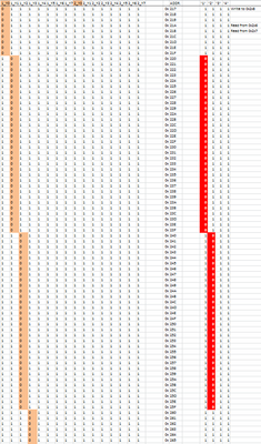
Also, I have to mention, that there are four resources that can be controlled:
- AY itself (with all of its registers, modes and so on)
- PCM DAC
- Joystick 1
- Joystick 2
PCM DAC can only be written and has "length" of one byte.
Each joystick can only by read and each of those also has "length" of one byte.
Almost 5 a.m. here... Seems like I have almost no time to sleep before my job. Oh, well.


![2018-10-27 20-14-49.mkv_snapshot_22.51_[2018.10.28_03.51.36].jpg](./thumbs/29431_532457d29354be0ced88ae34770eedb3/2018-10-27%2020-14-49.mkv_snapshot_22.51_%5B2018.10.28_03.51.36%5D.jpg)
![2018-10-27 20-14-49.mkv_snapshot_25.09_[2018.10.28_03.52.15].jpg](./thumbs/29431_bd02d2794ff9b3d7579f07784927e499/2018-10-27%2020-14-49.mkv_snapshot_25.09_%5B2018.10.28_03.52.15%5D.jpg)
![2018-10-27 20-14-49.mkv_snapshot_24.25_[2018.10.28_03.52.06].jpg](./thumbs/29431_6195fc6079268f8c3e26f7fe406ad460/2018-10-27%2020-14-49.mkv_snapshot_24.25_%5B2018.10.28_03.52.06%5D.jpg)
![2018-10-27 20-14-49.mkv_snapshot_23.08_[2018.10.28_03.51.47].jpg](./thumbs/29431_8d062ba2662ee7e54a0e47923f1b807c/2018-10-27%2020-14-49.mkv_snapshot_23.08_%5B2018.10.28_03.51.47%5D.jpg)