Deunan wrote:First lets check that reset signal before we start tracing it any further. Use a meter rather than probe, it's slow changing and fully controlled.
1) Check that the voltage on pin 11 of the 8284 clock generator (U91?) is above 3.5V at all times - I mean, just watch it for some 30s or so to make sure the PSU is outputting a stable PWR_GOOD.
Stable 4,7V
Deunan wrote:2) Then check that it drops to near 0V when you press the reset switch. To make sure the switch works.
Drops to 0,01V
Deunan wrote:3) Check pin 10 of the 8284, it should be the opposite of pin 11. In other words, close to 0V at all times except when the reset switch is pressed, then it should be at least 3.5V
It's 0,17V and then 4,18V with Reset depressed.
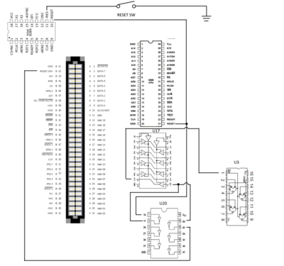
Deunan wrote:Assuming that's all good, find out where the ISA slot pin B02 is connected. It should be a pin on one of the '04 chips, but that can be anywhere on the mobo. Pin 10 of the 8284 should also be connected to the same '04 chip. Once you find those connections, also test the voltage on those '04 pins with and without reset being applied.
ISA B02 is connected to U20 '04 pin 12. It's 0,14V and then 3,75V with Reset depressed.
8284 pin 10 is not connected to U20 '04 pin 1. It's 0,17V and then 4,16V with Reset depressed.
Deunan wrote:Now, it should be possible to test the '373 chips. The rising voltage you've observed is most likely the chip heating up a bit, […]
Show full quote
Now, it should be possible to test the '373 chips. The rising voltage you've observed is most likely the chip heating up a bit, that's normal. The chip itself is a transparent latch and in this particular state it should just pass the logic level from inputs to outputs. There are 8 pairs, mapped like this (input->output):
3->2, 4->5, 7->6, 8->9, 13->12, 14->15, 17->16, 18->19
If in doubt, remember that inputs are tied to CPU socket and outputs are not. Also, preferably use a 100ohm (up to some 330 should work as well) resistor rather than a wire to short the inputs to ground. No need to connect them to 5V, TLL chip should default to high logic level by itself.
So, first check the voltage on all outputs. The actual value is not important as long as it represents a correct logic level. So lets add some margins and say below 0.6V is L, and above 3.5V is H. I'll use L/H instead of 0/1 as to not confuse logic level and voltage. Unless you see one output being considerably different voltage than others, then report that. Small differences (up to 0.2V or so) are OK.
In default state all output should be H. Then just use the resistor (or a wire) to bring each input to GND, and check if the output also went L. Test both '373 (U24, U25) that way.
Well, this part was tricky as they are crumped between ISA slot and CPU socket...
[#pinnumber] [default output voltage] -> [output voltage with input grounded with 100Ohm resistor]
U24
#19 3,82V -> 0,14V
#16 3,80V -> 0,14V
#15 3,81V -> 0,14V
#12 3,82V -> 0,13V
#9 3,83V -> 0,13V
#6 3,83V -> 0,13V
#5 3,80V -> 0,14V
#2 3,80V -> 0,14V
U25
#19 3,80V -> 0,14V
#16 3,80V -> 0,14V
#15 3,80V -> 0,14V
#12 3,85V -> 0,13V
#9 3,85V -> 0,13V
#6 3,80V -> 0,14V
#5 3,80V -> 0,14V
#2 3,80V -> 0,14V
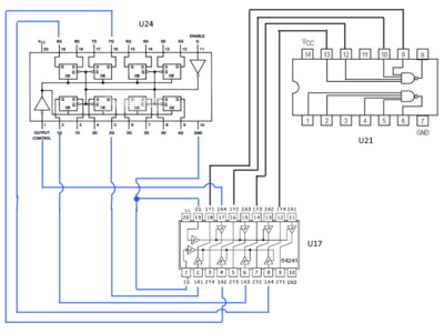
Deunan wrote:Next, remember that '20 gate (U21)? It's pins 9,10,12 and 13 should be connected to U24 pins 19,16,5,2. Except I don't know the exact order but it's not critical. Verify that pin 8 on U21 is L in default powered state. Then bring each of the following U24 pins 18,17,4,3 to GND with resistor, as above, and make sure the pin 8 on U21 goes H each time you do that. It's enough to test one by one, no need to test pin combinations or anything like that.
There is no connection between U21 or U86 (which is '20 as well) and U24 or U25.
U21#8 is green (L) and turns red (H) when pins 18,17,4,3 on U24 are grounded through resistor (one by one).
Deunan wrote:Now move to U50 '138 chip. It should be connected like this: U50#1 -> U24#12, U50#2 -> U24#6, U50#3 -> U24#15. If that is not the case, then see if these 3 pins (1,2 and 3) are connected to any other pins on U24, U25 or U15. Just to make sure I didn't get the wrong '138 chip. Again if not, then I guess there is another buffer chip in between and we'll have to find it.
No connections between U50#1/2/3 and U24 or U25 or U15 or U23 or U17 or U8(any pin) detected.
However there are connections like this to U48 '244 chip:
U50#1 -> U48#7
U50#2 -> U48#5
U50#3 -> U48#3
U24#6 -> U48#15
U24#9 -> U48#11
U24#10 -> U48#1 & #10
U24#12 -> U48#13
U24#15 -> U48#17
U24#20 -> U48#20
Also some pins on U25 '373 are connected to U43 '244
Also there is another '373 chip below U48 (marked U54) which is connected to U58 '245 below it
All these chips are in front of the ISA slots.