1TL866II can support VPP 18V and VCC 1.8V-6.5V, You don't have to worry about 12 volts. You can test it yourself with a blank chip.if it can not work,Please send me the screenshot of the error message,I'll report your problem to the manufacturer
He doesn't seem to understand that I'm wanting to know about 12 V to RP#, not Vpp. Perhaps my question wasn't clear enough, his English isn't good enough, the automated eBay English to Chinese translation isn't sufficient, or his knowledge is too limited. My message to him was:
1Intel E28F002BC and Micron MT28F002C1 both require that 12 V be passed to the RP# pin to unlock the boot block. Is the TL866IIplus able to supply 12 V to RP# to unlock the boot block? If not, the TL866IIplus cannot properly program these EEPROM chips. On the other hand, Intel E28F002BV and Micron MT28F002B1 chips (which are on the TL866IIplus support list) do not require 12 V to RP#. These EEPROMs can unlock the boot block with only 5 V to RP#. Please confirm if TL866IIplus can supply 12 V to RP# on the TSOP40 pinout (E28F002BC and MT28F002C1)?
Plan your life wisely, you'll be dead before you know it.
For the Batman board, FMUP is the supplied utility. So you think I need to follow the blind manual procedure I outlined previously? Or perhaps it automatically looks for _.BIO? That would be surprising since the newer VS440FX board needs to be directed to it with the /p flag.
I'm not entirely sure, but for the old motherboards, that's probably the only way, on the other hand, VS440FX maybe could pick up files in recovery mode automatically. This is what I found, regarding BIOS recovery for motherboards that were relevant in 1998:
1 BIOS Recovery
2
3Note: Not all standard Intel products support the Flash BIOS recovery feature. If your motherboard (for example, the Advanced/AS) does not have the recovery feature, ensure that you do not power down your system during a BIOS upgrade. This could corrupt the BIOS code. If your BIOS is left in an unusable and unrecoverable state, it will be necessary to contact the place of purchase.
4
5In the unlikely event that a FLASH upgrade is interrupted catastrophically, it is possible the BIOS may be left in an unusable state. Recovering from this condition requires the following steps (be sure a power supply and speaker have been attached to the board, and a floppy drive is connected as drive A):
6
7    1. Change Flash Recovery jumper to the recovery mode position (see note above; not all products have this feature)
8    2. Install the bootable upgrade diskette into drive A:
9    3. Reboot the system.
10    4. Because of the small amount of code available in the non-erasable boot block area, no video is available to direct the procedure. The procedure can be monitored by listening to the speaker and looking at the floppy drive LED. When the system beeps and the floppy drive LED is lit, the system is copying the recovery code into the FLASH device. As soon as the drive LED goes off, the recovery is complete.
11    5. Turn the system off
12    6. Change the Flash Recovery jumper back to the default position.
13    7. Leave the upgrade floppy in drive A: and turn the system on.
14    8. Continue with the original upgrade.
15
16Jumper locations can be found in the Technical Product Specification or on the "jumpers" page for each individual product.
17
18Updated: Monday, November 16, 1998
Recovery instructions implies, that no additional steps are required to start the BIOS recovery. Link
feipoa wrote:
I've attached the two BIOSes from user kixs. the NSSI created BIOS is only 64K, while the UNIFLASH created BIOS is only 128K. Does this make sense to you? Shouldn't it be closer to 256K? According to the UNIFLASH documentation, the boot block is automatically recorded starting with v1.33. I sent kixs version v1.40.
I had inspected both images. Image made using NSSI is just a decompressed BIOS copy from the shadow RAM and it's not entire, while image made using UNIFLASH seems legit, but its size is twice as small. From NSSI image I'd gathered, that kixs's motherboard is using 1.00.17.CS1 BIOS version. I tried to look for BIOS update utility of that particular version, so that I could compare image's structure with separate *.BIx files directly, but could not find it anywhere (file name for the update util. reqd. - 10017CS1.EXE). Still, compared 128KB image with 1.00.18.CS1 BIOS update files and its structure goes in this order: *.BI3 (most resembling)+boot block(dated 96-12-06)+*.BI2(most resembling), *.BI1 is absent completely and *.BIO is filled with FFs anyway.
Boot block in UNIFLASH's image is located at C000-10000 HEX address range (basically in the middle), I would not trust this image and I doubt that kixs's motherboard uses a 128KB FLASH chip.
Sedrosken mentioned, that he also has the VS440FX, you should ask him for help too, maybe he knows a way how to dump a 256KB image?
feipoa wrote:He doesn't seem to understand that I'm wanting to know about 12 V to RP#, not Vpp. Perhaps my question wasn't clear enough, his […] Show full quote
He doesn't seem to understand that I'm wanting to know about 12 V to RP#, not Vpp. Perhaps my question wasn't clear enough, his English isn't good enough, the automated eBay English to Chinese translation isn't sufficient, or his knowledge is too limited. My message to him was:
1Intel E28F002BC and Micron MT28F002C1 both require that 12 V be passed to the RP# pin to unlock the boot block. Is the TL866IIplus able to supply 12 V to RP# to unlock the boot block? If not, the TL866IIplus cannot properly program these EEPROM chips. On the other hand, Intel E28F002BV and Micron MT28F002B1 chips (which are on the TL866IIplus support list) do not require 12 V to RP#. These EEPROMs can unlock the boot block with only 5 V to RP#. Please confirm if TL866IIplus can supply 12 V to RP# on the TSOP40 pinout (E28F002BC and MT28F002C1)?
I'm not entirely sure, but for the old motherboards, that's probably the only way, on the other hand, VS440FX maybe could pick up files in recovery mode automatically. This is what I found, regarding BIOS recovery for motherboards that were relevant in 1998:
I've decided to hold off on the Batman's Revenge recovery procedure. If I have success with the VS440FX, I might reconsider. I'm generally not very lucky.
Stop torturing the distributors
lol, yeah, I'm done with this bloke. The manufacturer never returned my email inquiry, so I figured this was as close as I could get. The guys at Wellon tech support always returned my emails and added chips to the support list on request.
I had inspected both images....
Thank you! I've asked kixs which BIOS version is on his MB and he confirmed 1.00.17.CS1. I also sent Sedrosken a PM. Is there any value in requesting that kixs update the BIOS to 1.00.18.CS1?
Sounds like the code in the boot block doesn't update with the various BIOS updates? From your analysis of 1.00.18.CS1, it sounds like the bulk of the BIOS only needs 128 KB? Could one then correct the issue by adding FF paddings in the appropriate locations, re-positioning the address of the boot block code, and updating the checksum? Do you think Uniflash is altering the address of code based on FF's? I don't understand why the boot block would be moved. I assume the EEPROM itself has a specfic address where the boot block must be, so perhaps Uniflash doesn't support the particular EEPROM and is moving the boot block based on where the boot block is for a 1 Mbit chip?
EDIT: Unfortunately, the Intel E28F002BV chips didn't arrive today. Perhaps sometime this week then - tracking now says Aug 15.
EDIT2: At this stage, do you think it preferred to try flash your bootblock file, or the Uniflash kixs file?
EDIT3: Sedrosken is using 1.00.18.CS1 on his Gateway VS440FX board. This EEPROM is the same as my original, E28F002BCT80
You should also inspect Vpp and RP# pads on motherboard, maybe they constantly receive 12V.
At least in the off-state, Vpp and RP# do not receive 12 V. No other pad on the TSOP40A received 12 V.
Plan your life wisely, you'll be dead before you know it.
Is there any value in requesting that kixs update the BIOS to 1.00.18.CS1?
There's no point if UF returns 128KB images. According to UF1.40 documentation file, the 28F002 chip was never tested, nor 28F020, 28F004 was tested and it didn't work as it should, most likely 28F002 doesn't either.
13.0            What flash chips are supported by UniFlash ?
2-----------------------------------------------------------
3
4UniFlash supports the following flash chips:
5 * means tested and functional,
6 # means tested, but doesn't work the way it should,
7 unmarked chips are not tested (note that a lot of chips are very similar to
8 one another though, so if one of them works then the rest should work fine
9 too)
10
11,----------------------------------------------------------------------------,
12| Flash ROM                       | Size                                     |
13`---------------------------------|------------------------------------------'
14  Intel                           |
15  -----                           |
16  28F256(A)                       | 32KB
17  28F512                          | 64KB
18 *28F010                          | 128KB
19  28F020                          | 256KB
20 *28F001BX/BN-T                   | 128KB
21  28F001BX/BN-B                   | 128KB
22  28F002-T series                 | 256KB
23  28F002-B series                 | 256KB
24 #28F004-T series                 | 512KB
25  28F004-B series                 | 512KB
26  28F008-T series                 | 1024KB
27  28F008-B series                 | 1024KB
28  28F008SA                        | 1024KB
29  28F004Sx series                 | 512KB
30  28F008Sx series                 | 1024KB
31  28F016Sx series                 | 2048KB
32  28F016S5                        | 2048KB
33  28F004B3-T                      | 512KB
34  28F004B3-B                      | 512KB
35  28F008B3-T                      | 1024KB
36  28F008B3-B                      | 1024KB
37  28F016B3-T                      | 2048KB
38  28F016B3-B                      | 2048KB
39  28F320J5                        | 4096KB
40  28F320J3A                       | 4096KB
41  28F640J5                        | 8192KB
42  28F640J3A                       | 8192KB
43  28F128J3A                       | 16384KB
44 *82802AB (Firmware Hub)          | 512KB
45 *82802AC (Firmware Hub)          | 1024KB
46----------------------------------|-------------------------------------------
feipoa wrote:
Sounds like the code in the boot block doesn't update with the various BIOS updates?
That, or there was no necessity to update boot block untill the 18.CS1 version showed up.
feipoa wrote:
From your analysis of 1.00.18.CS1, it sounds like the bulk of the BIOS only needs 128 KB? Could one then correct the issue by adding FF paddings in the appropriate locations, re-positioning the address of the boot block code, and updating the checksum?
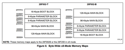
No, no, no, no, it would make more sense to guess the right order in which divided BIOS image from update util. should go and then try to stick them together. This is how a proper mem map should look like for that BIOS image (T prefix).
Sedrosken has BIOS version 1.00.18.CS1 on his VS440FX. Is there any value in having him attach the Uniflash created binary for his system?
Agreed - I wouldn't be probing the EEPROM pads with MM probes while powered up. If there wasn't a via, I'd solder a wire to the pad. Do you think knowing the voltage of Vpp and RP# while powered is important?
Sedrosken has BIOS version 1.00.18.CS1 on his VS440FX. Is there any value in having him attach the Uniflash created binary for his system?
No need.
feipoa wrote:
Do you think knowing the voltage of Vpp and RP# while powered is important?
RP# should be at 5V~, Vpp - anything but 12V~.
feipoa wrote:
The EEPROM's arrived today!
Hurry up with the boot block flashing, I want to see that MB POST 😁
By the way, that 16KB image is 100% a boot block. Check the last 16 bytes of that image, it has the far jump instruction (EA) with the segment and offset address of F000:C05B.
that 16KB image is 100% a boot block. Check the last 16 bytes of that image, it has the far jump instruction (EA) with the segment and offset address of F000:C05B.
Not sure what you want me to check? I'm not very familiar with BIOS binary code.
Sedrosken already sent me the Uniflash file of 1.00.18, so I've attached it for completeness.
I'll try to get to the EEPROMs tonight. With school out, my kids seem to stay awake forever. They didn't stop screaming until 2:30 AM last night; it was horrible.
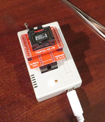
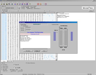
1) write the bootblock bin you attached to E28F002BVT60 using TL866IIplus using TSOP40A adapter
2) solder E28F002BVT60 to motherboard
3) set recovery jumper on VS440FX and power on
4) ensure that the 1.00.18 recovery diskette is inserted
5) wait until no more diskette activity, wait 2 more minutes, power down, put recovery jumper back to normal, reboot
6) voila?
Or is there any benefit to powering up the system without the recovery jumper set once the EEPROM is soldered on? Perhaps the power LED will stop flashing?
Plan your life wisely, you'll be dead before you know it.
Wait a minute... I measured Vpp in the off-state again today and it is connected to 12 V. RP# is not connected to 12 V, nor 5 V. Either I was mistaken the last time I measured Vpp, or there is an intermittent short. Does this new found knowledge alter the next course of action?
EDIT: power-on test, Vpp is 12.33 V. I went to measure RP# and the board (or power supply) started making a hissing sound, then the system shut down. I unplugged everything, waited 5 minutes, plugged the PSU back and hit power, the CPU fan spun up, but after a few seconds, there was this hissing sound. I thought it was the CPU fan, so I unplugged it, but the hissing sound was still there. It got louder, and fearing that I might get a cap blown in my face, I turned it off. Again, I'm not sure if it is the PSU, or the MB, but considering the issues, I'm guessing the MB. I checked for shorts on those electrolytic surface mount caps, but didn't find any shorts.
EDIT2: The capacitor just below the CPU socket measures only 30 ohms across its terminals. I'm guessing this is the source of the hiss? Perhaps I'll remove the cap and measure the resistance on the solder pads... EDIT3: the solder pads without the cap are also 30 ohms. EDIT4: swapped the PSU, don't hear a hiss so far. I'm going to let it run for a few minutes. Still not sure what to do about 12 V on Vpp. Perhaps a default response when no BIOS detected? EDIT5: I followed the traces for Vpp and it is intentionally hard-wired direct to 12 V, and not through a pull-up resistor. I guess I will continue with programming the *BV chip now.
EDIT6: Another user with the board also confirms 30 ohms across the resistor I removed and that Vpp on the EEPROM is wired to 12 V.
Plan your life wisely, you'll be dead before you know it.
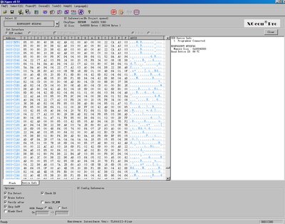
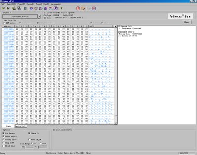
I inserted the VS440FX's original BIOS, the E28F002BCT80 into the TL866IIplus programmer. Attached is an image of "missing pins". The programmer doesn't have chip support for the E28F002BCT, but rather the E28F002BVT. Not surprising that the programmer software says that pin 12, which is N/C on the *BC chip and WP# on the *BV chip, is not connected. Also curious though is that it says pin 11, which is Vpp is a non-connect. Did the Vpp pin get burned out? Or is it connected internally on the *BC chip compared to the *BV chip, which is causing the programmer not to detect it? I had hoped to make a copy of whatever BIOS was on the original *BC chip, but this isn't going to happen.
I tried pushing my finger on the EEPROM while it was in the adapter, and that didn't help for these two pins. It helped for when pin 7 showed a disconnect, but not for pins 10 & 11. Too much flux on the pin to make contact? Probably not.
I also tried the Micron MT28F002B1 setting, but the outcome was the same.
So the FLASH chip is set permanently to be in write/erase mode? How odd... Hissing noise usually indicates, that PSU is overloaded. Did resistances change between GND and the rest of PSU lines on MB, compared to those on the 1st post?
I decided to read what was on the NOS E28F002BVT60. They don't come blanked?
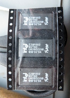
Interesting, those FLASH chips that you've bought are NOS, no doubt, but they are preprogrammed for production. According to the image, those chips were supposed to be used in the Ericsson DCT1900 comunications system. I bet those things cost huge sum of money back in the 90's.
Attaching boot blocks from kixs's and Sedrosken's VS440FX MB BIOSes, for archiving purposes:
SSTV2 wrote:Interesting, those FLASH chips that you've bought are NOS, no doubt, but they are preprogrammed for production. According to the […] Show full quote
feipoa wrote:
I decided to read what was on the NOS E28F002BVT60. They don't come blanked?
Interesting, those FLASH chips that you've bought are NOS, no doubt, but they are preprogrammed for production. According to the image, those chips were supposed to be used in the Ericsson DCT1900 comunications system. I bet those things cost huge sum of money back in the 90's.
Attaching boot blocks from kixs's and Sedrosken's VS440FX MB BIOSes, for archiving purposes:
kixs's_VS440FX_boot_block_96-06-12.zip
Sedrosken's_VS440FX_boot_block_96-05-21.zip
[/b][Emphasis mine]
1.00.18.CS1_98-08-28.zip
I wonder, what difference does BB's version make.
I find it interesting that despite my having the newest BIOS installed, I have the oldest boot block of the three. It works just fine, I can boot from CD natively even. Something had to have been updated because with the older BIOS, I couldn't do that.
So the FLASH chip is set permanently to be in write/erase mode? How odd... Hissing noise usually indicates, that PSU is overloaded. Did resistances change between GND and the rest of PSU lines on MB, compared to those on the 1st post?
Is that so it can write ESCD configuration data? Where is ESCD stored in that BIOS block diagram you attached?
I didn't check this systematically yesterday. I will check this evening when the the owls and raccoons roam.
Looks like flashing the motherboard never changes the boot block. This is part of its protection mechanism. But makes me wonder, though, why does Intel update the boot block code between revisions if it doesn't get implemented? Must only be for new motherboards being pushed out. Intel must have some software/programmer combination which combines their BIOS fragments before writing the EEPROM.
Is there any value in aligning the boot block code to the appropriate addresses on those backups you made so that one could easily program them? I can imagine if I fail with the .18 boot block, that I'd probably try another.
Plan your life wisely, you'll be dead before you know it.
I should note that when I had the original BIOS soldered on that -5 V to GND was a short, but now it is an open circuit (or greater than the 50 M-ohm limit of my multi-meter). Recall that 5 V to GND was 60 ohms with the old BIOS, then became 1.4 K-ohm once removed. -5 V to GND is now OC instead of SC.
Plan your life wisely, you'll be dead before you know it.
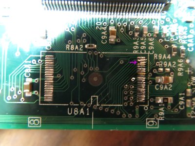
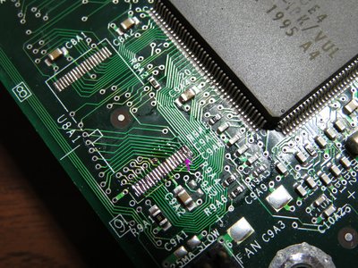
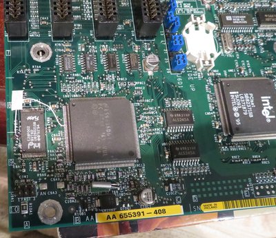
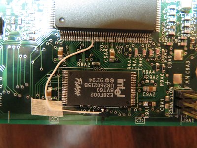
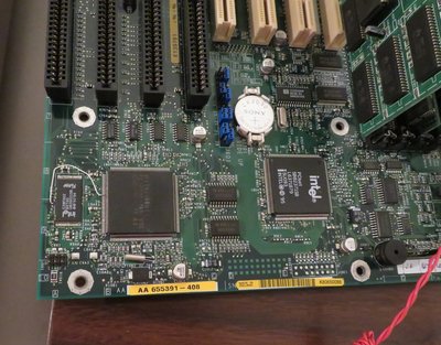
I have soldered on the boot block programmed E28F002BV EEPROM. Unfortunately, I ripped off part of the pin (arrow in photos) and had to run an external patch wire. I don't have much experience soldering on such tight spacing - perhaps my smallest tip isn't quite small enough, so I had some issues with solder blobs. Using a spring loaded, hand held solder socker simply provides too much kickback and uplifted a few pads. I was able to get them back in place, but one of the pads broke of half-way.
Nonetheless, the best approach to get this IC back on was to pre-coat all the pins with a just the right amount of solder, then align and hold the EEPROM in place with masking tape. Then bring the soldering iron to each pin and let it reflow onto the EEPROM pins. On my first attempt, I didn't have any solder on the TSOP40 pads and tried to add solder to each pin as I went a long. After about 8 chips in, I started getting fat solder bridges, and this is when I brought out the spring-loaded solder sucker (ooops!).
Anyway, I'll try to fire this up tomorrow. I assume I'm to go right into recovery mode?
EDIT: If I get it working, I'll probably take the tape off and tack the wire down with a dab of epoxy. Also, I had to use these 10x magnifier glasses to solder the TSOP40 leads. I noticed only one burn scab on my nose this morning, though I swear I burned myself twice.
Plan your life wisely, you'll be dead before you know it.
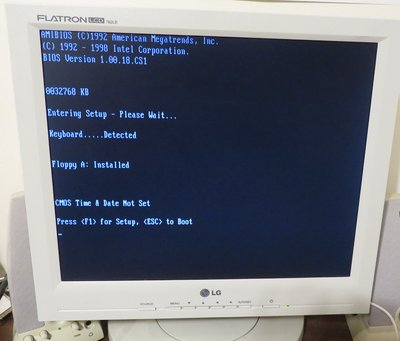
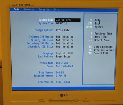
I was really skeptical when I powered it up in recovery mode because there was no diskette activity for about 40 seconds. I was about to turn it off, then all of a sudden the diskette started reading. Once diskette activity ceased, the diskette light was on solid for what felt like 2 minutes, then it finally went off. I placed the BIOS normal jumper back on, then rebooted. System asked me for a password, so you also must set the disable password jumper, turn on, then off, then on again with the password jumper back to default. I'm attaching some photo proof that it works.
I also removed the tape on the jumper wire as the fix looks less obvious this way. I should get some of that green 32 AWG wire that I see some manufactures use on motherboard for fixes. It is really inconspicuous. At least I think it is 32 AWG. The white kynar cladded wire shown in the photos is 30 AWG and the wire on MB fixes I've seen appears smaller.
Many thanks to sedrosken and kixs for copying their BIOSes and especially to SSTV2 for his invaluable insight and resolve.
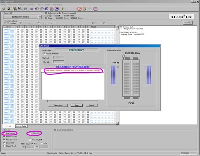
For the record, I contacted the the eBay distributor about not being able to use the *BC EEPROM on the TL866IIplus programmer - he was in fact the one who claimed the *BC EEPROM was supported prior to purchase. He did get back to me what a somewhat dubious solution, to uncheck "pin detect" and "check ID" on the programmer software. Unfortunately, I do not have a working *BC EEPROM to confirm if this method actually works, but I've attached a screenshot of the result with my faulty *BC EEPROM. Overcurrent protection! External Short!
The closest literal translation in English would be every honor. It's used as an exclamation when congratulating someone or expressing amazement over someone's accomplishments.