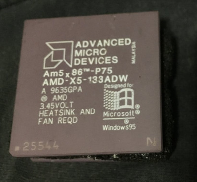
The other two AMD P75 CPUs (both 5x86 marked and X5-133ADW) are also 25544.
The 5x86 cores down-binned to DX4s should that code as well (as ph4nt0m said), and I think all the 16kB cache versions of the AM486 are 5x86s.
Interestingly, the date code (or I think it's the date code) seems to be the newest on that "486 DX5" at 9738CPA.
The other two are 9606APD and 9645APA.
It's also possible my particular 486DX5 is a fake/remarked chip, but it's really well done if it is. It's engraved rather than printed and the 25544 model number is slightly shallower than either of the others (also black like one of the other two, the 3rd example has uncolored engraving there). If it is a fake/remark, the original could've been printed/painted and had those markings scrubbed with little ceramic surface removed (just polished) and not lose some of the thickness required for the older Intel 486SX remarks that were pretty common (SX25 to SX33), but I'm not sure.
The font looks really similar to the older engraving used on some AM386 makes, but without the flat-topped capital A. Plus the numerical font doesn't have that LED/LCD/floro tube style digital matrix look that the 386 markings have.
It's really precise, small, good looking engraving though. (and definitely a functional CPU, one I'll have to try out more when I have a later model 486 board fully working ... and either sorted out with trial and error or a proper manual, as I haven't found one for my Acorp branded SiS 495 based one yet)
If those late model DX4-100s do share that same model number, doing those sorts of remarked chips would be pretty simple and systems/benchmarks would detect them the same.
OTOH there's one thing nagging at me here:
ph4nt0m wrote on 2020-04-04, 17:52:That's not a surprise. AMD sold many 5x86 chips labelled simply as […]
Show full quote
That's not a surprise. AMD sold many 5x86 chips labelled simply as
Am486DX4-100
A80486DX4-100SV8B
package 25544
They still had 16Kb cache and could be overclocked to 160MHz easily. Original 500nm SV8B package 25398 couldn't do that.
I'd thought the 16kB DX4s were marked DX4-100SV16B. That's certainly what I'm finding pictures of right now as well, along with the 25544 numbering.
And DX4-100 and -120 SV8B models seem to be 25398 chips.
http://www.chipdb.org/img-amd-a80486dx4-100sv16b-247.htm
There's also some marked NV8T and 25253, which must be an earlier revision, apparently also using the .5 micron process, but with write-through rather than write-back cache.
http://www.cpu-world.com/CPUs/80486/AMD-A8048 … X4-100NV8T.html
The DX4 120 was apparently made in both the write-back and write through forms as well, and share those part/mask numbers with the 100. (also some DX2 66 and 80 parts share the NV8T or V8T and 25253 numbers, and those parts also might support both 2x and 3x multipliers)
I have a pair of AMD DX2-66 chips that appear to be 5V ones (or don't have 3V written on them) and lack a suffix after the 66. Both are 24361. I'm not sure what process they use, but maybe the same old .7 micron one used for the AM386 and 1x multiplier 486s. (which would make sense to compete with Intel's .8 micron BiCMOS DX2-66)
Those .5 micron parts are also interesting in the category for potentially tolerating 5V power. If nothing else, they should handle it better than the .35 micron ones that are definitely known to have fairly short lifespans at that. (as some 200 MHz 5x86 overclocking attempts and/or successes have ended in)
That and it should be the same process AMD used for the early K5 parts, and makes me wonder if AMD could've gotten away with bumping the voltage a bit on those to help with yields, at least if improved cooling methods were also introduced. (though between voltage regulation and heat, more like 4.0V which was the normal setting used on Nexgen's .5 and .35 micron parts in proprietary boards) I haven't seen any references to Socket 5 boards with overvolting support like that either, to try with actual Socket 5 parts, though given how limited typical heatsink+fan set-ups were up through 1996 that's also not too surprising and probably would've been more interesting for overclocking Intel CPUs anyway. (given they ran cooler and already often had a bit of overclocking headroom at 3.4 or 3.5 volts)
Hmm, though given AMD had trouble even getting 90-100 MHz K5s out early on, and given how warm 3.52V 6x86 PR-150 and 166 (120-133 MHz) chips ran, 4.0V might not have been that strange. Unless they were specifically trying to avoid some of the mixed PR Cyrix was getting over those heat and power consumption issues. (plus they avoided supporting the 75 MHz bus speed that Cyrix jumped to even though AMD's 1.5 and 1.75 multiplier settings should've been quite appealing, and I imagine it was at least somewhat popular back then to bump 105 MHz K5 PR-150s up to 112.5 MHz and get performance generally beyond the PR-166)
Since AMD may have avoided actually marking 5x86 chips as x5 160 (4x40 MHz) to avoid cutting in on K5 sales (and likewise avoided 3x50 ratings), it seems like that conflict would've also been avoided by voltage bumping the K5 into a higher performance bracket. (that and doing additional yield management by releasing a 1x66 MHz model of K5 priced closer to the 5x86, though the faster FSB should put it ahead of the K5 75 and 5x86 P75 parts alike for a fair number of things)
It seems some early model K5s, at least the two '5k86' 75 MHz examples I have do have a 1x multiplier setting mapped to Intel's and Cyrix's 2x jumper configuration). Both also seem to go OK at 1x83 MHz 3.5V, but not 95 and I don't have any 90 MHz capable boards to try. Cyrix's 1x multiplier is more well known on the 6x86, and I'd assume was an appealing option for some very early adopters with 80 MHz (2x 40) rated models, and maybe even some situations with the 2x50 MHz ones, especially on boards with larger L2 cache and/or fast DRAM performance. (the 50 MHz case also usually means 25 MHz PCI bus too, though 40 MHz PCI with 40 MHz FSB would be one plus point for the 80 MHz part ... and the 3x multiplier setting for that matter, if you had one of those unusual boards with 40 MHz FSB + 1x PCI)
Well that, and I'd think 1x66 MHz socket-4 compatible upgrade modules would also be appealing. Assuming Cyrix and AMD didn't want to actually run their parts at 5V or even bother manufacturing socket 4 packages, they could've gone the soldered-on-board voltage regulator + pin adapter route like some 486 and 5x86 upgrade boards did. (and having slower, but non-buggy FPUs and faster 16-bit code and/or general ALU performance would seem like selling points) Granted, AMD was so late to market that the Cx6x86 is far more relevant there. (Cyrix's early, 1995 production 6x86s would've been still relevant for Socket 4 systems)
I mean ... I could take some of my Socket 5 and 7 CPUs with 1x multiplier settings and pit them against some of the faster 486s here and see if there's even any relevance (compared to people building fast Socket 4 systems back in 1995/96 ... not so much those who actually had Socket 4 boards). Though I'm tempted to see how that ISA bottleneck issue pans out too. I have one or two FX based Socket 5 or 7 boards (or they're marked socket 7 on the socket, but not full socket 7 spec) that might be worth comparing ISA performance on. None of the early (fast for the time) SiS based Socket 5 boards to compare either on my end.
That supposedly very-slow OPTi Socket 4 pentium chipset with VLB slots would be interesting to compare too, including on the VLB vs ISA performance differences, or if it actually does better with ISA performance than the same cards do on faster, PCI based boards. (though I guess Intel's and SiS's Socket 4 chipsets would also be relevant for comparing there, and ALi's for that matter)


