VOGONS


AMD K7 "goldfinger" cloning thread

Topic actions

Reply 60 of 260, by debs3759

User metadata
Rank Oldbie
Rank
Oldbie

That was fast! I look forward to buying one if it tests working 😀

See my graphics card database at www.gpuzoo.com
Constantly being worked on. Feel free to message me with any corrections or details of cards you would like me to research and add.

Reply 61 of 260, by gex85

User metadata
Rank Member
Rank
Member

Well, the good news first: I didn't destroy any hardware in the process (yet) 😁

The not-so-good news: It does not work as expected. I tried it on my 550 MHz Athlon on two different boards (EP-7KXA with Award BIOS, FIC SD11 with AMI BIOS). The results are slightly different, but similar:

All settings for even multiplicators result in 94 MHz FSB frequency and 1.0x multiplicator = 94 MHz on the Epox board and in 350 MHz on the FIC board.
All settings for odd multiplicators result in 44 MHz FSB frequency and 1.0x multiplicator = 44 MHz on the Epox board and in 300 MHz on the FIC board.
Both boards won't boot with VCore settings below 1.70V although the CPU is rated at 1.60V (this might as well be due to the resistor value that is slightly different than on the original GFD).

This is a bit disappointing, but hey, it's a prototype after all 😉
Tomorrow I'll try to do some more investigation.

Edit: I did not verify any of the frequencies yet, it’s just what the BIOS reports...

My retro computers

Reply 62 of 260, by wiretap

User metadata
Rank Oldbie
Rank
Oldbie

Did you set the dip switches both toward each other for ON, and both away from each other for OFF? I think the resistor needed to be 2k ohms.

My Github
Circuit Board Repair Manuals

Reply 63 of 260, by gex85

User metadata
Rank Member
Rank
Member
wiretap wrote on 2021-02-22, 21:26:

Did you set the dip switches both toward each other for ON, and both away from each other for OFF? I think the resistor needed to be 2k ohms.

Yes, sure... I set all switches 100% correctly as described in the manual.
Will see if I have a 2k resistor at hand...

My retro computers

Reply 64 of 260, by gbeirn

User metadata
Rank Member
Rank
Member

That is odd behavior. I'm still waiting on my PCBs to arrive.

Here is the (mostly) depopulated Ninja device if someone wants to produce in Kicad. Should be self explanatory but I can answer questions or test continuity further if need be.

Attachments

Reply 65 of 260, by gbeirn

User metadata
Rank Member
Rank
Member

Good news: the pcb finally arrived.

Bad news: I can’t locate any of my slot a motherboards. The only one I have in my possession currently is the ABit one I bought on eBay with the Ninja Goldfinger device. It needs a recap and I don’t have all the caps I need.

So: does anyone want to test one of these? I can send you the parts or assemble it, your choice. If it works, you can pay pal me some money to cover the costs, if not, we’ll go back to the drawing board.

Maybe 2-3 people, preferably in the US. In the mean time I’ll get what I need to recap the Abit board and try and track down my others.

Reply 66 of 260, by gbeirn

User metadata
Rank Member
Rank
Member

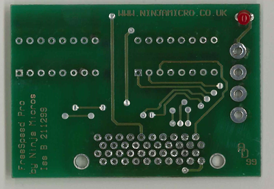
Here is what I have found out and what I think is going on.

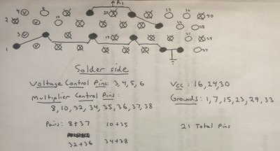
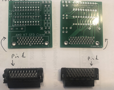
I drew a hand diagram but realized I labeled the pins based on looking at the back of the connector (the solder side). On the golden fingers connector there are 4 pins that control voltage - 16 possible states or voltages. There are actually 8 pins that control the multiplier but they are redundant and duplicated. Meaning each pair of pins should both be set to the same state (high or low). That's why the Northwind device only has 4 switches for a multiplier and the sets of pins are tied together with the traces on the connector. My Ninja device is an older style and uses all the pins separately resulting in needing many more DIP switches but I verified looking through the tables I have that those same pairs or switches and pins are always pulled in the same way (i.e., one is high and so is the other and vice versa).

I think the problem is the DIP switch is sometimes left floating. The very top DIP (SW1) when the switches are in the up position are pulling high through the 2K resistor and the associated power pins on the connector. When the SW1 is down this is obliviously disconnected. However the bottom DIP (SW2) should then be pulling the pins to ground but the problem is the bottom row of pins on the bottom DIP aren't connected to anything. The only one that has a connection is M3. M3 leads to several pins on the connector all tied together.

I think jumpering or soldering (when looking at the back of the device) the 8 bottom rightmost DIP switch pins together should get the device working. I can't verify this because as I mentioned previously I can't find the boards I need. I'm guessing maybe these are connected together under the DIP switch on the original and we can't see that in the photos we have. It's also possible there are other pins on the connector that need to be tied together like on my Ninja and are maybe on the Northwind just under the connector and we can't see it, I think this is less likely though.

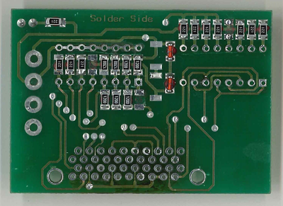
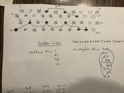
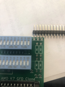
In the attached picture I have figured out what pins do what. This is based on the Ninja Freespeed device but is mostly applicable to wiretap's PCB.

The pins are numbered when looking at the solder side. Pins marked with a 'V' are the ones that control the voltage states. Ones with a 'X' are unused. The empty circles are the multiplier pins, again 8 of them but (using my labeling) 40/2 , 29/13 , 20/19, and 9/8 are redundant. They can be tied together so that you only need 4 DIP switches. I have no idea what would happen for example if you pulled pin 40 high and pin 2 low.

The top 3 dark circles are connected to together and go to the 2K ohm resistor. The bottom dark circles are interesting. On the Ninja all of these are connected together and do not go to any where else on the PCB. The Ninja has a power connector so everything is pulled to ground through the power connector pins. The three with an '*' above them are not connected to anything on wiretap's prototype but are tied together on Ninja. These are the pins that go to M3 on wiretap's board and I think should go to the other bottom DIP pins.

Thoughts anyone?

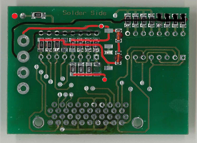
Edit, I'm tired and may not be explaining myself well. I am proposing the green line in the second photo attached to this.

Attachments

Reply 67 of 260, by wiretap

User metadata
Rank Oldbie
Rank
Oldbie

You are correct. Look here, it's a trace I missed because I thought everything was on the rear of the board. Bottom left next to the gold finger header. It goes from ground, between the cap (supposed to be resistor) and to the bottom row of dip switches.

exM7Hwe.jpg

This can be corrected on existing boards with one wire connected to a ground pin on the gold finger connector, then just solder bridge the bottom 1-8 pins on the lower dip switch. Now to find which one is a ground on the gold finger header..

Edit: it looks like on the original version, they have lower DIP switch position 2 hooked to ground on the rear. 2-8 are likely bridged to ground on the front through that pin under the DIP casing. Then the first lower dip switch position 1 or 2 goes on the front side to ground and ties in to ground again with the rest? Kind of weird, because it seems like they could just bridge all 8 on the front under the bottom row header and not need a trace on the front going to the gold finger header. Who knows, maybe they do have it that way. Since position 2 seems to already be tied to ground, bridging the bottom row of positions 1-8 on the lower dip switch should do it.

It may be prudent to measure position 2 lower pin on the lower dip with a multimeter to validate it is ground when the PC is on.

My Github
Circuit Board Repair Manuals

Reply 68 of 260, by wiretap

User metadata
Rank Oldbie
Rank
Oldbie

Per http://web.archive.org/web/20010220225123/htt … lockingpg3.html

io58I5O.jpg

It does match up with the lower dip switch position 2 bottom pin going to ground. So, those lower pins of the bottom dip switch position 1 through 8 can be tied to ground. Pin 40 also appears to be a ground, which is connected as well per the original Northwind GFD.

My Github
Circuit Board Repair Manuals

Reply 69 of 260, by wiretap

User metadata
Rank Oldbie
Rank
Oldbie

New schematic for Feb 28th, 2021. KiCAD gerbers and project file attached. If you don't want a new board, you can tie the lower dip switch lower pins in positions 1-8 to each other. This can easily be accomplished with solder bridging or a stripped solid core wire tied across them and soldered in place. Please note, this is experimental since we can't see exactly where that front trace goes and we are assuming based on other designs.

evfOI2J.jpg

VVXutsz.jpg

Attachments

My Github
Circuit Board Repair Manuals

Reply 70 of 260, by gbeirn

User metadata
Rank Member
Rank
Member

Awesome! Here is my redrawn sketch of the solder side of the connector. The only think that has changed is the numbering of the pins is now correct.

Pin 1 is the bottom left and you count up and over so pin 40 is in the top right side.

Attachments

Reply 71 of 260, by wiretap

User metadata
Rank Oldbie
Rank
Oldbie

The only thing I'm unsure of on that table is how they have the pins numbered. Look at he the KiCAD project PCB for how the pins are numbered per the official footprint and manufacturing.

Also, I'm tracing out the whole schematic and making a net for the Ninjamicro for how it maps to KiCAD pin assignments. That will be next, and for sure successful since we have all the traces mapped 100% correct.

My Github
Circuit Board Repair Manuals

Reply 72 of 260, by gbeirn

User metadata
Rank Member
Rank
Member

I agree on the pin numbering. I aligned my second drawing to match theirs but that now doesn’t match your numbers on the schematic. We are both saying the same thing and the connections are correct from what I can tell .

If I look at the data sheets for the connector, what they call pin 1 is completely different as well 🤣.

Attachments

Reply 73 of 260, by gbeirn

User metadata
Rank Member
Rank
Member

I think your reversed engineered design should work now. It’s been super helpful to me in figuring out the Ninja and why there are so many extra DIP switches.

There is one glaring design flaw and that’s just with the original: if the user moves the DIP switches in the wrong direction, VCC can be shorted to ground.

I think if you replaced the two DIP switches with 1 SPDT bank that would eliminate that possibility. That might make trace routing difficult however I’m not sure.

Reply 74 of 260, by gbeirn

User metadata
Rank Member
Rank
Member

Also wiretap, would you mind adjusting the pin spacing for the cache control? Make it the same standard as the DIP. 2.54mm I think? Makes assembly using the headers easier.

Attachments

Reply 75 of 260, by wiretap

User metadata
Rank Oldbie
Rank
Oldbie

On the original design they just used wires soldered into there, no pin headers. But once we determine if this design with the grounds is fully working, I'll clean up the PCB and issue a final design. I'll probably also add a warning on the PCB to never flip both rows of 1-8 to the up position, as you'd be shorting the CPU internally.

My Github
Circuit Board Repair Manuals

Reply 76 of 260, by gex85

User metadata
Rank Member
Rank
Member

Great work guys. I didn't have much time for retro computing activities during the past week, but I had already noticed that the lower dip switch had suspiciously few traces going to it.
I think tomorrow evening I'll find some time to apply the fix to the GFD that I have already assembled.

My retro computers

Reply 77 of 260, by t4ker

User metadata
Rank Newbie
Rank
Newbie

I really love your passion to build a goldfinger clone and your knowledge about reverse engineering. Hopefully it will work with the last fixes - fingers crossed 😀.

Reply 78 of 260, by wiretap

User metadata
Rank Oldbie
Rank
Oldbie

Ninjamicro layout. This will make working in KiCAD much easier. Thanks @gbeirn. --- I'll need those diodes measured to see what type they are. Have to make sure we have the right ones for the voltage drop. All the resistors we know already from the markings. I'm guessing the diodes are 1N4148's (LL4148) with a 0.7V drop each.

Nqatwtt.jpg

Last edited by wiretap on 2021-03-01, 02:56. Edited 2 times in total.

My Github
Circuit Board Repair Manuals

Reply 79 of 260, by greasemonkey90s

User metadata
Rank Member
Rank
Member

Im in for one of these. awesome work guys. I have a mint asus k7m dieing to invest more time on slot a. just not a fan of the limitation of cpu frequency without one of these. Currently only have a athlon 800 pluto though but dont mind testing. Sign me up for a finished assembled one . Not sure who in the states i have to pm to invest.

Last edited by greasemonkey90s on 2021-03-01, 18:33. Edited 1 time in total.