VOGONS


Lucky Star LS486 rev D and 3V CPU's

Topic actions

First post, by carlostex

User metadata
Rank l33t
Rank
l33t

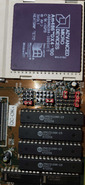
Roughly one month ago the VR on my LS486 rev D literally blew. Not only i heard a popping noise i saw smoke rising from VR area and suddenly i see the damn thing crack!

So i ordered LM317 and L7805 VR's from ebay. I desoldered the cracked VR from the board and tried to boot it with a 5V CPU. No matter what i tried the damn thing wouldn't boot. So i thought the 1000uf 10V capacitor that is near the VR was also dead. So i ordered same voltage same rating japanese capacitors. Yesterday i soldered both capacitor and the LM317 VR.

Board is ALIVE AGAIN!!! At least with 5V CPU's. With 3V no dice. So i checked all the tips of VR with multimeter and when i set the board to 3V CPU's the center tip is in fact delivering around 3.05V. I guess this is insufficient to power the 3.3V CPU's i tried. When i actually powerup, i can see the lights of the keyboard blinking, but there is no beeps, no POST, nothing.

Now i noticed that the original VR on board is marked as TIP107. So i google it and it does report as a power transistor instead of a voltage regulator.

I haven't tried the L7805 yet and i'm probably gonna try it tomorrow, but i've been wondering if i really do need a TIP107. As i don't understand these electronic thingies i hope someone can tell me the difference between them.

Waiting anxiously for the experts answers on my problem.

Thanks in advance

Reply 1 of 20, by luckybob

User metadata
Rank l33t
Rank
l33t

pics?

but if the cap didn't look bad and replacing it, fixed a problem, it stands to reason the whole power regulator unit needs service.

The problem is, its hard to diagnose these issues without being hands on. Usually an oscilloscope is required to check ripple and for voltage spikes.

It is a mistake to think you can solve any major problems just with potatoes.

Reply 2 of 20, by Old Thrashbarg

User metadata
Rank Oldbie
Rank
Oldbie

You can't just randomly replace a transistor with a voltage regulator... they're two entirely different things. It won't work, and it may even fry something. If it had a TIP107, then you need to put another TIP107 in its place, and hope you didn't kill anything else when you tried the LM317.

Reply 4 of 20, by feipoa

User metadata
Rank l33t++
Rank
l33t++

Some motherboards use power transistors instead of voltage regulators for the CPU's 3.3-3.6 V supply. They are usually cheaper. I think this is what PCChips did. While you may be able to use your existing power transistor, you would need to check the pin-outs of the power transistor and of the cracked voltage regulator and decide which SMD resistors on the motherboard need to be altered. Note that I have not personally bothered to check the spec sheets of the TIP107 and the LM317; I am only offering general advise. Now, if the pin-outs are totally different, then you'd have to move your circuit into 3D. Usually designing a voltage regulator around a power transistor requires more circuit components and probably won't work as a drop-in replacement as you were hoping. The 3.05 V is somewhat promising in that maybe you just need to change the set resistors on the motherboard, but I personally wouldn't want to bugger anything else up. I have pretty itchy hands with this type of work and would still order the diret replacement part.

3.05 V is insufficient for most 486 CPUs. Even some CPUs which claim to work at 3.3 V needed 3.35 V in my experience.

Plan your life wisely, you'll be dead before you know it.

Reply 5 of 20, by Old Thrashbarg

User metadata
Rank Oldbie
Rank
Oldbie

While you may be able to use your existing power transistor,

That's the thing, though... while there is often a certain amount of leeway in substituting transistors (and even different pinouts can be dealt with easily enough), the LM317 and 7805 are not simple power transistors, they're standalone linear voltage regulators. They require a quite different circuit design. And actually, to be completely accurate, the TIP107 isn't a simple transistor either, it's a Darlington pair.

And even if you were to somehow modify the board's circuitry to work with the different components, those regulators still have a much lower current capacity than the TIP107 and probably wouldn't handle the load.

Getting a measured 3.05V with the LM317 was just dumb luck, nothing more. It doesn't mean it was anywhere close to working properly.

Reply 6 of 20, by carlostex

User metadata
Rank l33t
Rank
l33t
Old Thrashbarg wrote:

... those regulators still have a much lower current capacity than the TIP107 and probably wouldn't handle the load.

Yeah i guess that is very much true. I didn't mentioned that the first time i actually tested a 3V it actually booted. I used an AMD 486 DX4 100NV8T and i did set it only to DX2 66 and it actually booted... until the system completely locked up while it was testing the RAM... It did not boot a 3V CPU anymore. All CPU's tested in this experience are still alive.

However it seems i was lucky. I won't powerup the board anymore until i desolder the LM317 and solder one of the TIP107's i ordered.

EDIT: I just went following feipoa's advice and went to check the datasheets. The TIP107 can peak a total of 15A of current against only 1.5A of the LM317.

I learned my lesson. 😅

Reply 7 of 20, by carlostex

User metadata
Rank l33t
Rank
l33t

OK. First of all i want to thank all who've replied this thread. I learned my lesson, and it should have a purpose for everybody else.

TIP107's have arrived yesterday. So today just as i arrived from work, desoldered the LM317 and soldered a TIP107 in its place. Booted with a 5V CPU success!!! Booted with a 3V AMD 486 (NV8T) success again. Board is up and running again!

@feipoa
The Lucky Star LS486 rev D has both the SiS chipsets and it does have a PCI bus divider. No PS/2 mouse port though... 🙁

Reply 8 of 20, by feipoa

User metadata
Rank l33t++
Rank
l33t++
carlostex wrote:
OK. First of all i want to thank all who've replied this thread. I learned my lesson, and it should have a purpose for everybody […]
Show full quote

OK. First of all i want to thank all who've replied this thread. I learned my lesson, and it should have a purpose for everybody else.

TIP107's have arrived yesterday. So today just as i arrived from work, desoldered the LM317 and soldered a TIP107 in its place. Booted with a 5V CPU success!!! Booted with a 3V AMD 486 (NV8T) success again. Board is up and running again!

@feipoa
The Lucky Star LS486 rev D has both the SiS chipsets and it does have a PCI bus divider. No PS/2 mouse port though... :(

I'm glad you were able to get it working. Doing it right the first time is often the easiest approach.

It looks as if JP16 controls the 1/2 PCI frequency. Are you able to trace where this jumper goes? If so, which pins of the chipset or BIOS does the jumper trace to? I am wondering if jumping the same locations on the Zida Tomato 4DPS will also cut the PCI frequency in half on that board. The 4DPS has the advantage of the PS/2 port and non-soldered cache. However, LS486 rev C and F used socketed cache.

Plan your life wisely, you'll be dead before you know it.

Reply 9 of 20, by carlostex

User metadata
Rank l33t
Rank
l33t

I think i found it!!!! The 1 and 2 JP16 pins connect to a MX8325-1MC IC! I just checked the datasheet!

http://www.datasheetarchive.com/indexer.php?f … =user-highscore#

I'm almost pretty sure that the JP16 pin1 connects to pin 9 of MX8325 but i'm not sure where pin 2 connects.

Reply 10 of 20, by feipoa

User metadata
Rank l33t++
Rank
l33t++

Ok, thank you for this information. I'll look at this in more detail when I have time. The 4DPS board uses MX8310-01PC clock generator, so I'll have to see how much work is required to adapt this change. I couldn't find the spec sheet on the MX8310-01PC, so I'd need to measure the output with a scope.

Plan your life wisely, you'll be dead before you know it.

Reply 11 of 20, by rad

User metadata
Rank Newbie
Rank
Newbie

Do you know what exactly is the purpose of this jumper (PCI divider)? Will setting it to 1/2 will actually make 33MHz CPUCLK setting work to 66MHz and therefore divide PCI to 33MHz? I can't see any purpose of this divider with just 25/33/40 BUS Clock.

Reply 12 of 20, by jesolo

User metadata
Rank l33t
Rank
l33t
rad wrote:

Do you know what exactly is the purpose of this jumper (PCI divider)? Will setting it to 1/2 will actually make 33MHz CPUCLK setting work to 66MHz and therefore divide PCI to 33MHz? I can't see any purpose of this divider with just 25/33/40 BUS Clock.

No, it's actually the other way around.
The standard specification of the PCI bus is to run at a maximum speed of 33 MHz.
On older motherboards, the PCI bus ran at the same speed as the external front side bus (FSB) of the CPU.

When you install a CPU that runs at 40 or 50 MHz FSB, you are actually overclocking your PCI bus as well, which is outside of the standard specification.
Most PCI graphics cards tend to run OK up to 40 MHz but, I've read posts that it can give trouble on network and IDE controller cards if you exceed the standard specification of 33 MHz.
The purpose of the PCI divider is to underclock your PCI bus so that it doesn't exceed the maximum speed of 33 MHz.

Unfortunately, in the case of this motherboard, there is only a divider of 2 (40 MHz ÷ 2 = 20 MHz & 50 MHz ÷ 2 = 25 MHz), which is way below the standard specification.
This means that your PCI graphics card (or any PCI card) will run at sub optimal speed.

However, later motherboards kept the PCI bus at 33 MHz, regardless of the FSB.
Based on the MX8325-1MC datasheet, it appears that it does make provision to run the PCI clock at the standard frequency but, I don't think it is implemented on the LS486 rev D (a quick check in the BIOS setup might confirm this but, my LS486 rev D motherboard isn't currently installed).

On a different note.
I noticed that, although not documented in the manual, there are soldering points right next to the keyboard connector (labelled CN3).
I have a suspicion that this might be for a PS/2 connector but, even if I could solder the connectors to the motherboard, I'm not sure whether there is actually a PS/2 controller on board.

Reply 13 of 20, by carlostex

User metadata
Rank l33t
Rank
l33t
jesolo wrote:

On a different note.
I noticed that, although not documented in the manual, there are soldering points right next to the keyboard connector (labelled CN3).
I have a suspicion that this might be for a PS/2 connector but, even if I could solder the connectors to the motherboard, I'm not sure whether there is actually a PS/2 controller on board.

I don't think so, but there are also solder pads for a keyboard controller chip like an Holtek one, which includes PS/2 support.

Reply 14 of 20, by rad

User metadata
Rank Newbie
Rank
Newbie

Guys I have Lucky Star LS486E rev.C2 motherboard. This one seems to have also undocumented jumpers for enabling CPU/BUS clock divider. As you properly mentioned it is just 1:1 or 1:2, but this is what is perfect for me.

The manual of the motherboard says that it supports only 25, 33 and 40 MHz with 3 jumpers one above another. BUT I've found out that the wiring of the 3 jumpers go directly into the S(2:0) input signals of MX8325-1MC clock generator. Actually this board (SIS496/497) is capable of 66Mhz FSB! In order to enable it you've to close all 3 jumpers to produce TTL level of 000 for S(2:) which is actually inverted state of the jumpers (i.e. TTL 0 = Closed Jumper; TTL 1 = Open Jumper). There is another undocumented jumper called JP19 which switches the output of the clock generator to either CPUCLK or CPUCLK/2.

So I was able to start and power on, test and (for now seems stable under DOS since I don't use anything else at the moment) my IBM-100HF is now benching at 133MHz (2x66)! I'll post another thread with very interesting results and screenshots, which differ somehow from those in UMC boards.

Reply 15 of 20, by sparky4

User metadata
Rank Newbie
Rank
Newbie
rad wrote on 2015-04-30, 13:16:

Guys I have Lucky Star LS486E rev.C2 motherboard. This one seems to have also undocumented jumpers for enabling CPU/BUS clock divider. As you properly mentioned it is just 1:1 or 1:2, but this is what is perfect for me.

The manual of the motherboard says that it supports only 25, 33 and 40 MHz with 3 jumpers one above another. BUT I've found out that the wiring of the 3 jumpers go directly into the S(2:0) input signals of MX8325-1MC clock generator. Actually this board (SIS496/497) is capable of 66Mhz FSB! In order to enable it you've to close all 3 jumpers to produce TTL level of 000 for S(2:) which is actually inverted state of the jumpers (i.e. TTL 0 = Closed Jumper; TTL 1 = Open Jumper). There is another undocumented jumper called JP19 which switches the output of the clock generator to either CPUCLK or CPUCLK/2.

So I was able to start and power on, test and (for now seems stable under DOS since I don't use anything else at the moment) my IBM-100HF is now benching at 133MHz (2x66)! I'll post another thread with very interesting results and screenshots, which differ somehow from those in UMC boards.

is it possible to enable 66mHz on the rev D board. i have one

wwww

Reply 16 of 20, by feipoa

User metadata
Rank l33t++
Rank
l33t++

Yes. You need to solder on a missing jumper header at JP15, pins 5-6, which is normally open. When closed, you have access to 55, 60, 66, and 75 MHz FSB's.

Plan your life wisely, you'll be dead before you know it.

Reply 17 of 20, by sparky4

User metadata
Rank Newbie
Rank
Newbie

you mean like this? i dont see space for pin 6?

Attachments

  • 20230805_110255.jpg
    Filename
    20230805_110255.jpg
    File size
    377.32 KiB
    Views
    945 views
    File comment
    close up of jumpers
    File license
    Public domain

wwww

Reply 18 of 20, by sparky4

User metadata
Rank Newbie
Rank
Newbie

here is the full board

Attachments

  • 20230805_111719.jpg
    Filename
    20230805_111719.jpg
    File size
    17.55 KiB
    Views
    939 views
    File comment
    full board
    File license
    Public domain

wwww

Reply 19 of 20, by feipoa

User metadata
Rank l33t++
Rank
l33t++

My LS-486E Rev.D has two banks of SOJ SRAM. Yours has one bank of DIP SRAM. I'm not familiar with your Rev.D.

Plan your life wisely, you'll be dead before you know it.