Reply 420 of 1184, by Sphere478

Rank
l33t++
- Rank
- l33t++
Yeah, I am thinking I can add pads that people don’t have to use if they don’t want to.
Yeah, I am thinking I can add pads that people don’t have to use if they don’t want to.
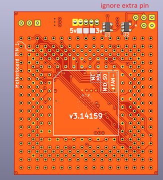
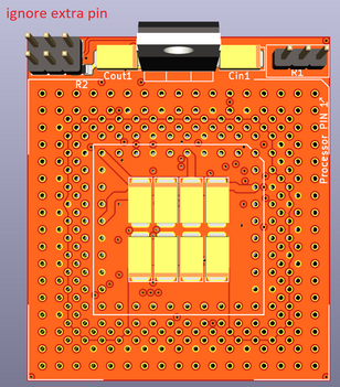
v3.14159
How does this look?
There is a courtyard violation between cout and r2, but it is fine. we can ignore. 😀
the 3d model shows 6 pins but there are only 5 holes don't worry.
Out of curiosity I overlayed the socket 1/2/3 tweaker over this interposer. It seems to be a match… grounds and power are in the same locations..
Think the tweaker could be stacked on top of this adapter to install typical socket 3 4/586 class cpus?
This brings up the question though,
Is memw something that should be added to the socket 1/2/3 tweaker?
This is a passive adapter. You can't just drop a 486 into a 386 socket...they're not bus compatible, you need some extra "glue". Reverse engineering the Transcomputer modules would be a good place to start if that's something you wanted to pursue.
"Will the highways on the internets become more few?" -Gee Dubya
V'Ger XT|Upgraded AT|Ultimate 386|Super VL/EISA 486|SMP VL/EISA Pentium
Sphere478 wrote on 2022-10-17, 22:41:v3.14159 CPUInterposer386-486 beta 3.14159.zip How does this look? […]
v3.14159
CPUInterposer386-486 beta 3.14159.zip
How does this look?There is a courtyard violation between cout and r2, but it is fine. we can ignore. 😀
the 3d model shows 6 pins but there are only 5 holes don't worry.
Sorry, took me a while to find the time to look into this with KiCad. Addition looks perfect though, thanks!
Blavius wrote on 2022-10-25, 18:48:Sphere478 wrote on 2022-10-17, 22:41:v3.14159 CPUInterposer386-486 beta 3.14159.zip How does this look? […]
v3.14159
CPUInterposer386-486 beta 3.14159.zip
How does this look?There is a courtyard violation between cout and r2, but it is fine. we can ignore. 😀
the 3d model shows 6 pins but there are only 5 holes don't worry.
Sorry, took me a while to find the time to look into this with KiCad. Addition looks perfect though, thanks!
Excellent! 😀
Btw, do you have part numbers/links? I can add part numbers to the silk. That makes it easier on people ordering. 😀
Absolutely;
U1 = M74VHC1GT14DTT1G -VCx
U2 = M74VHC1GT32DTT1G-VNx
I ordered both from AliExpress.
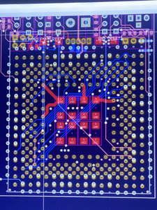
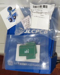
Box arrived from JLCPCB. Contains the beta SXL2 boards and some 3dfx SLI boards I tacked onto the order.
Plan your life wisely, you'll be dead before you know it.
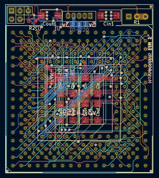
I just had to check a few pins to determine that relying on JLCPCB's auto-detection and default settings was a poor decision. R1's trimmer pins 2 and 3 aren't connected, neither are D20 and D9. D11 and D19 are OK. I didn't bother to check the other 164 pins.
Plan your life wisely, you'll be dead before you know it.
>If I select 4-layer, the cost is $28. If I select 6 layer, cost is $86.
So you pushed 6 layer gerber, but ordered 4 layer? and they actually routed only 4 layers? brilliant 😁 Cha bu duo chef's kiss
haha, I was going off the intelligence I received, although against my gut. Apparently they always come out correct in the end. Debunked.
It ended up being $14 CAD for 10 pieces, not $28, since 4-layer lets you do everything in HASL (lead). I also had the concern that if their auto analysing script detects 4 layer when it should be 6 layer, then I could also run the risk of forcing a 6 layer and still receiving 4 layer. I suspect there's some incomplete fundamentals in the gerbers which is enabling JLCPCB to miss layers. I'm hoping JLCPCB will let us know what that is.
Plan your life wisely, you'll be dead before you know it.
feipoa wrote on 2022-10-28, 10:14:haha, I was going off the intelligence I received, although against my gut. Apparently they always come out correct in the end. Debunked.
It ended up being $14 CAD for 10 pieces, not $28, since 4-layer lets you do everything in HASL (lead). I also had the concern that if their auto analysing script detects 4 layer when it should be 6 layer, then I could also run the risk of forcing a 6 layer and still receiving 4 layer. I suspect there's some incomplete fundamentals in the gerbers which is enabling JLCPCB to miss layers. I'm hoping JLCPCB will let us know what that is.
Well it was worth a try. They should refund you and now we all know moving forward which was something we needed the answer to.
In the meanwhile you can order the new version, get a refund and test if you can actually physically solder it 😀
Use their online chat feature to talk to them.
I can assure you, without any doubt, that soldering won't be an issue. I realise a few of you have had trouble visualising this process, so I will get you some step-by-step photos of how this can be soldered with a simple iron. Solder paste not needed. Hot air not needed. Finagling not needed. If you spend 20 minutes thinking about how this can be done, as I did years back, I'm sure you'd come to a similar conclusion.
Even if I had a proper male-to-male PGA132 (did they ever exist?), it could still be soldered easily just that the very outer edge of the PGA132 would need to be surface soldered from the top side, rather than the bottom. However, since we're using single rows, it is even easier.
Of more concern for me right now is the distance from some of the PGA-132 holes to the smaller vias. Sphere, what is the smallest gap here?
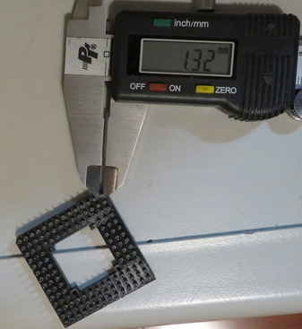
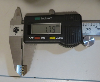
I was looking at my male-to-male machine pins and it looks like the head of these have a wider diameter than that of standard PGA socket pins. Standard PGA sockets have a 1.32 mm diameter, while my gold male-to-male pins has 1.79 mm. I hadn't noticed this.
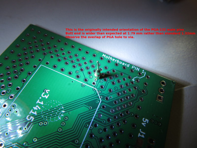
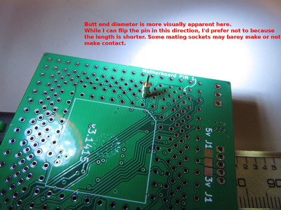
There's probably about a dozen vias that are affected. The easy solution is flip the row header around and use the solder-end for the exposed-end and the exposed-end (the end you would normally used to make soft contact) for solder-end. I'm not a fan of this because you cannot push the final product as far into the motherboard's socket and you won't be able to use socket removal tools with the ends flipped. When I was test pressing the flipped end into a socket, I can see it just barely clicks in, then it cannot go in another further. On some other sockets, it may barely not click in. With the ends flipped the proper direction, you get full penetration with confidence it won't come out.
Another idea I had was to use some extra conformal acrylic coating around those vias before I soldered or to put some kapton tape over the vias.
Ideally, though, I'd find those male-to-male gold headers with normal width butt stops, but I suspect this will be a challenge.
Plan your life wisely, you'll be dead before you know it.
I won’t be in front of a laptop for possibly almost a week, another user could measure those clearances for you sooner in the kicad file. But spacing should be about the same as socket 5/7/370 spacing and pad edge to pad edge I don’t recall but probably similar to socket 5/7/370
As for via clearance, it will have to be measured.
A tiny drop of nail polish over sensitive spots might help 😀 or conformal coating, but pcb varnish is probably the best to use. If you can figure out what to order. Paints and conformal coatings may melt from solder heat. The varnish won’t if you get the right stuff.
I see your dilemma there.
Suggest maybe not fully seating the top socket, (leaving space between the board and pin cups) or using tall pin sockets. They have some with legs that are longer. You could space it so that the pins didn’t protrude on the back. That would help
As for bottom socket to motherboard, perhaps using pins from a old socket 370 celeron or something? Or order some? (Check pin length/thickness)
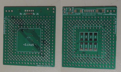
That pcb looks beautiful btw :p nice to see all that work in physical form :p
Btw, resistor legs don’t work well for pins, though it is a prototype option. They bend very easily. Might not be the best idea for data pins though. 🤔 though 30/72 pin simms seemed to do okay with tinned contacts…
Yeah, PCB looks slick. It is smaller than the VRM interposer I'm using on my stacked SXL2-66 configuration.
Concerning the issue with the oversize butt ends of the pin headers, I was thinking I might just use something flat and thin to help offset the pin heads while soldering. Perhaps a piece of paper, or even something a little thicker like a photograph. This would let the butt-end hover over the PCB about 250 microns, or 0.25 mm. It will definately add time and inconvenience to the job. I've looked on few platforms for pins with a smaller butt-end, but either they all are oversized, or the photo doesn't properly convey the image. Nonetheless, at this stage (pre-testing), I'm not going to spent any more time on it. That is a fine-tuning step and we aren't there yet.
I left a message with JLCPCB and they sent the issue to someone to look into.
Plan your life wisely, you'll be dead before you know it.
feipoa wrote on 2022-10-28, 23:33:I left a message with JLCPCB and they sent the issue to someone to look into.
How's their English? I've never had to deal with their support before
Pretty bad usually haha but eventually you get the message through.


