Reply 860 of 1184, by Sphere478

Rank
l33t++
- Rank
- l33t++
Oh, wild!
If they use standard 386 pga chips, I don’t see why this interposer wouldn’t work other than bios support.
Feiopa? Thoughts?
Oh, wild!
If they use standard 386 pga chips, I don’t see why this interposer wouldn’t work other than bios support.
Feiopa? Thoughts?
I personally haven't tried an SXL on anything as old as an 8088 with an accelerator card. I would recommend that you first try it out with a standard PGA-132 DLC. if that works, try with a standard PGA-132 SXL. Then try SXL2. If the SXL2 works in clock doubled mode, I don't see any reason why the custom PGA-168 interposer wouldn't work. Have you tried a regular DLC/SXL?
Plan your life wisely, you'll be dead before you know it.
Looky what I found in the mailbox 😲
For anyone waiting for results, we are waiting on Feiopa. I currently don’t have the rest of the parts to assemble this right now.
But it looks perfect as far as I can see.
I managed to get this order in before the $2 promo ended. Is why I ordered it 🤣.
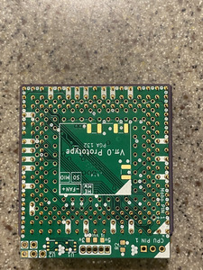
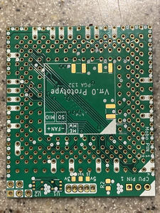
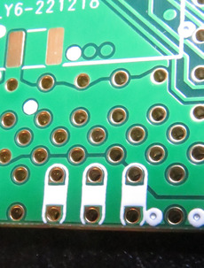
This shows the corrected round holes.
Seems to me that the vias with the squared ends would be slightly more ideal for soldering SMD caps to. Why are the PCBs with rounded holes the correct ones from your viewpoint?
Edit: Did JLCPCB provide any warning before they ended the promotion? When I chatted with them, they acted like it would be around for quite some time and there would be ample warning. Then *poof*
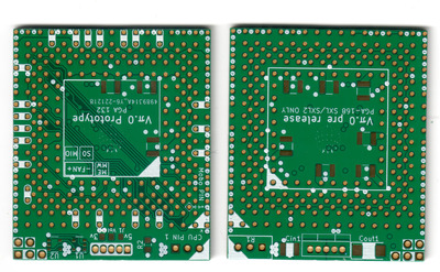
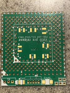
Dimensions: 4.2 mm x 4.9 mm. This is quite small. For comparison, my BL3 hack for PGA132 is 4.0 mm x 4.0 mm.
Plan your life wisely, you'll be dead before you know it.
feipoa wrote on 2023-01-26, 02:54:Seems to me that the vias with the squared ends would be slightly more ideal for soldering SMD caps to. Why are the PCBs with ro […]
Seems to me that the vias with the squared ends would be slightly more ideal for soldering SMD caps to. Why are the PCBs with rounded holes the correct ones from your viewpoint?
Edit: Did JLCPCB provide any warning before they ended the promotion? When I chatted with them, they acted like it would be around for quite some time and there would be ample warning. Then *poof*
SXL2_interposer_alpha2_scan.jpg
Dimensions: 4.2 mm x 4.9 mm. This is quite small. For comparison, my BL3 hack for PGA132 is 4.0 mm x 4.0 mm.
None of the pcbs came in with flat on one side pads. This was the whole problem. But they clearanced the flood like they were D shaped even though they weren’t. So the only things that happened from trying to make them D shaped were things that didn’t help us. So I went back to round pads (since that was all they could make) compare to yours, you’ll probably see what I mean.
I saw no warning from
Jlcpcb. For promo
Yes, :p this is about as small as is possible :p!
I keep staring at it but I don't see the problem. Am I getting elderly?
Plan your life wisely, you'll be dead before you know it.
feipoa wrote on 2023-01-26, 03:32:I keep staring at it but I don't see the problem. Am I getting elderly?
Your pads I assume are round but they clearanced the flood and silk like they are D shaped. (We have the same pads, but you have less silk, and less flood) ergo, no point.
Your scanned image is kinda hard to interpret on the pads. Look at your pads under a microscope, and report back.
On the pci 3.3v adapter I tried to use the same setup and the pads came in round. Not the expected D shape. I provided pictures of this problem earlier in the thread.
If somehow you ended up with D shaped pads for sure, then let me know, because then yet again jlc has thrown a curveball sending me round (on the 3.3v adapter) and you D shaped (on the sxl2 interposer).
My pads for the surface mount capacitors at the location of the PGA pins are are D-shaped. It looks pretty clear to me on the scanned image I provided. Try zooming in. I've also looked at the pads under a 10x jewellers eyepiece. They are D-shaped.
Plan your life wisely, you'll be dead before you know it.
Okay. It appears jlc decided to manufacture yours as it was sent to them. In which case, cary on, all good.
On my 3.3v adapter. They did not do this. Pads came in O shaped not D shaped
The question now becomes, wether or not they will continue to manufacture it correctly with subsequent orders?
So we now have two versions shown one with O one with D
Sphere478 wrote on 2023-01-26, 03:54:Okay. It appears jlc decided to manufacture yours as it was sent to them. In which case, cary on, all good. […]
Okay. It appears jlc decided to manufacture yours as it was sent to them. In which case, cary on, all good.
On my 3.3v adapter. They did not do this. Pads came in O shaped not D shaped
The question now becomes, wether or not they will continue to manufacture it correctly with subsequent orders?
So we now have two versions shown one with O one with D
Well, with the interposer being kind of an OverDrive part, O and D are pretty suitable 😉
Please use the "quote" option if asking questions to what I write - it will really up the chances of me noticing 😀
feipoa wrote on 2023-01-26, 02:54:SXL2_interposer_alpha2_scan.jpg
Is it just me, or does this scan indeed show a D shaped soldermask opening around round pads (as sphere suggested)? It also looks like all the squared pads (for the connectors) came out round, albeit with a squared soldermask opening.
Then, the scan looks as if all through-holes have become pads also and all the copper pads for the Us, etc. aren't even there...?
Or is that all the scanned image running tricks on me?
MJay99 wrote on 2023-01-26, 08:15:Is it just me, or does this scan indeed show a D shaped soldermask opening around round pads (as sphere suggested)? It also look […]
feipoa wrote on 2023-01-26, 02:54:SXL2_interposer_alpha2_scan.jpg
Is it just me, or does this scan indeed show a D shaped soldermask opening around round pads (as sphere suggested)? It also looks like all the squared pads (for the connectors) came out round, albeit with a squared soldermask opening.
Then, the scan looks as if all through-holes have become pads also and all the copper pads for the Us, etc. aren't even there...?Or is that all the scanned image running tricks on me?
missing holes for the trees! 😀
Feiopa says his came in correct and I believe him.
It was just annoying that they messed it up on my 3.3v pci adapters.
I ordered and got a round version (as ordered) so mine was correct for what I sent them.
You guys talk amongst yourselves if you want to use the round version or the D shaped version.
If jlc messes up again that would be undesirable. Because we will have sacrificed copper flood and mask for nothing.
Your call. I can see merit either way. But we need to decide now before next revision.
None of these have copper pads for SMD components between pins (referring to the bar shaped white silkscreen). You need to know the technical terms for PCB.
Mask is whole area of UV curable of any colour includling semitransparent mask of PCB to insulate top and bottom also to cover any unnecessary tracks and vias so solder is not allowed to soldered except select unmasked areas. Inter-layer insulation are related to the PCB substance to build internal layers of tracks and power planes, Silkscreen is for calling out component locations and component outlines, jumper naming and connector names, but never used to insulate, universally white. Vias is though hole without opening or have opening to inter-connect layers, and can be soldered where designed for, there are two types of vias, one is not solderable due to mask, while select vias is solderable.
Pads is 100% surface mount only, which is a area of flat copper areas for solder bordered by mask either not or outlined by silkscreen with location marking (U3, C3 etc). Pads is universally interconnected via tracks and vias of any width depending on power current requirements, even pad to pad only.
The PCB maker vendors do have tomes of design guidelines too and is not unlike any good PCB designers have books and online guidelines on doing this correctly.
And feipoa's is SMD version while your sphere478's is through hole.
What is going on?
PS: These custom boards made so far, top and bottom mask is not transparent including layers to show the tracks like other boards we are used to see and is easier to troubleshoot if you can see tracks plus sign of quality.
Edge connectors are improperly masked, they are not pads. The edge connectors has to be 100% unmasked and protected with hard plating for wear and corrosion resistance.
Cheers,
Great Northern aka Canada.
Thanks for the clarifications 😀 The D shaped pads on the thru holes are only on one layer which is why it felt more appropriate to call them singular as it didn’t describe the entire thru hole stack. They were made using copper flood and mask on one layer to create and expose them. Feiopa requested the silk in these areas as a extra layer of protection from his soldering iron as he had been having issues with the mask scratching off, and that makes sense. I do think it will help. I understand that normally you rely only on the mask alone. Honestly, I think the round thru holes are fine for attaching these capacitors but feiopa and others were very adamant about having them this shape. They actually wanted them to be larger, but wasn’t able to reasonably accommodate. So compromised.
Edge connectors?
Feiopa’s is not a smd. It is a thru hole. His scanner is playing tricks on you 😀
There aren’t very many surface tracks on this interposer there are some visible on the back side in middle though.
Feiopa, suggest posting pics again with a cell phone so elements show up better. The scanned image is confusing everyone 🤣.
Btw, couldn’t resist doing a mock-up 😁
Yes the scanned images are really hard to interprete if you don't know.
What appears to be solid pads where holes are supposed to be must be light reflected within the holes while the scanning was going on.
Had to have several looks on it, too, until I recognized what was what (even the vias seem to be closed/non-existent because of the "greened" light reflections from the solder mask inside them).
The actual pads beeing the darker brown areas and the golden "pads" beeing through holes.
Wouldn't hurt to "correct" these with actual photos since it's tricking everyone reading here very easily.
feipoa wrote on 2023-01-20, 12:03:I personally haven't tried an SXL on anything as old as an 8088 with an accelerator card. I would recommend that you first try it out with a standard PGA-132 DLC. if that works, try with a standard PGA-132 SXL. Then try SXL2. If the SXL2 works in clock doubled mode, I don't see any reason why the custom PGA-168 interposer wouldn't work. Have you tried a regular DLC/SXL?
Thanks so for the advice the inboard is currently running with a Cyrix cx486drx2 20/40 clock doubled Cyrix 386/486 132pin so I’ve every confidence in it working.
Looking forward to you guys getting this finalised - been watching this thread a long time
Mike
Mike1978, if it works with the DRx2 there's a good chance it will work with the SXL2. Sometimes the SXL2 is slightly more problematic with certain DMA SCSI controllers.
Another view of the D-pads. I'm surprised there is so much interest in these pads now. Solder mask is quite the distance from the pads. hmm...
Plan your life wisely, you'll be dead before you know it.
It seems jlc didn’t line up that silk very well. Oh well, some is better than none. Be careful with the iron 😀
