Reply 180 of 1184, by maxtherabbit
Rank
l33t
- Rank
- l33t
I'll be damned, looks like you got them up line up with an overlap huh. Nice work
I'll be damned, looks like you got them up line up with an overlap huh. Nice work
Aerion wrote on 2021-01-18, 16:22:Interesting thread about the upgrade with this cpu. Unfortunately on some boards there is not enough space around the 386 socket to place a PGA-168.
Yeah, depends on the particular motherboard and where the PGA is placed. Obviously the QFP144 variant of the SXL2-66 was preferred for this reason, but not sure where to source those.
Aerion wrote on 2021-01-18, 16:22:It's sure that the pins FLT # & MEMW # are not used? It would be good to check this against your interposer.
I don't have the Powerleap interposer which came natively with the PGA-168 version of the SXL2-66. I only have the QFP144 version w/SXL2-66 and the PGA168 version with SXL2-50 at 5V. I'm pretty sure I checked FLT# and MEMW# for the interposers I do have, with information buried in the text. The TI 486SXL databook also talks about these pins. MEMW# should be brought out to a header on the PCB for boards which need this connected to the ISA slot.
The SXL2-66 has the cache flush circuit built into it and that is what the MEMW# jumper header is for. Even if a board doesn't have the flush circuit and doesn't work with the MEMW# method (which is for serial level 2 cache), I have found that the software method to flush the cache (BARB) has almost zero negative impact on performance. I quantified it at one point and I recall it being only a few realtics on DOOM.
Leave FLT# floating. There is no FLT# on PGA-132. FLT# contains an internal pull-up to avoid and active low condition.
Plan your life wisely, you'll be dead before you know it.
Amazing thread. I’m in awe at the cool stuff you guys are doing.
Has anyone played with socket 5/7 stuff?
I would love to make a few socket 7 interposers for k6 2/3+ and tillamook.
maxtherabbit wrote on 2021-01-18, 16:56:I'll be damned, looks like you got them up line up with an overlap huh. Nice work
The pins of the header & socket must be shortened so that it fits properly on the PCB (Z-axis)...
As far as I can see, MEMW# doesn't have an internal pullup resistor. When not in use, it should be an external resistor at 3.6V. That would be a 3-pin header with GND(1) - MEMW #(2) - 3.6V(3). With a jumper on position 2 & 3, MEMW # would be inactive. Signal GND & MEMW# then goes to the mainboard via a cable. Both wires are twisted. Correct so far?
Niemand ist nutzlos, er kann immer noch als schlechtes Beispiel dienen...
Aerion wrote on 2021-01-19, 05:20:maxtherabbit wrote on 2021-01-18, 16:56:I'll be damned, looks like you got them up line up with an overlap huh. Nice work
The pins of the header & socket have to be shortened so that it fits properly on the PCB...
Obviously but it's a fit in the XY plane which is impressive
Aerion, do you have access to the TI486SXL databook? On page 5-2, section 5.1.2, table 5-1 lists inputs which are internally connected to pullup/down resistors. Unused pins with pullup/down do not require connection to external pullup/down resistors. MEMW# and FLT# are internally connected to pullup resistors on the both the QFP144 and PGA168 version of the SXL.
The databook also warns against adding external pullup/downs to NC pins.
The jumper block on the interposer should be for MEMW#, GND, 5V. GND & 5V are for a fan.
A second jumper block or even a mini-DIP could be used to set discrete voltage values if not using a trimmer, e.g. 3.5, 3.6, 3.7, 3.8, 3.9, 4.0 V.
Plan your life wisely, you'll be dead before you know it.
I had to search for the databook for a while before I found it. Now I have an overview of the signals.
Why do you need voltages over 3.6v? Maybe you will overclock the CPU with more than 33MHz?
A thermal design should be considered for the voltage regulator. Do you have a preferred VR type?
More parts increase the PCB dimensions and signal routing becomes more complicated. Decoupling capacitors should also be present on the VCC pins.
Niemand ist nutzlos, er kann immer noch als schlechtes Beispiel dienen...
Aerion:
The answers to your questions are contained in the body of this thread. I suggest reading through the thread in detail as the answers previously noted are likely to be more well thought out than what I can come up with on the spot now; human memory fades quickly.
Yes, overclocking. Discussed previously.
Yes, decoupling needed. Discussed previously.
Many 386 boards run stock at 40 MHz, so plan for a minimum of 2x40 MHz (80 MHz) and a maximum of 2x50 MHz (100 MHz). What voltage is needed at 2x50 MHz? That's what the variable VRM is for. Trimmer, mini-DIP, mini-jumper, etc. My QFP144 runs fine at 80 MHz, so the PGA168 likely will as well. This was also discussed previously.
VRM - discussed previously. I had overspec'd an LDO VRM with modern parts, MIC29302WT, however the Powerleap unit uses EZ1086, which may or may not be sufficient at x volts and 100 MHz. We will need to estimate the CPUs current draw at 100 MHz and, say, 4 V max. If I recall, the datasheet only goes up to 50 MHz at 3.3 V.
Plan your life wisely, you'll be dead before you know it.
The first study for PGA-168 without placing the parts:
I will publish the study for the QFP-144 on occasion.
Niemand ist nutzlos, er kann immer noch als schlechtes Beispiel dienen...
Aerion, nice work! Some comments thus far:
If you were to rotate the VRM by 90 degrees and place it towards the bottom, would you be able to fit in one of these mini DIP switches under the CPU? See the mini-DIP SW in the Trinity Works module here: download/file.php?id=50039&mode=view
Scratch that - an even better suggestion would be to place the DIP SW on the very bottom of the PCB. This way the user wouldn't have to pull out the CPU to adjust the CPU voltage.
After further thought, since we are going to have an exposed header, it might be good to have the FLT# pin brought out next to the GND pin header. FLT#, when grounded, would allow the SXL2-66 chip to be disabled, thus preventing the need to remove it from the motherboard if the user wanted to use an on-motherboard soldered-on CPU.
I'm curious why you think we need to have 5V and GND next to MEMW#?
I would arrange a 4-pin header like this: Vcc, MEMW#, GND, FLT#. Note that I've placed Vcc on the header, not 5.0V. This Vcc (3.6V) header will be helpful for the user to measure the CPU voltage with a multimeter.
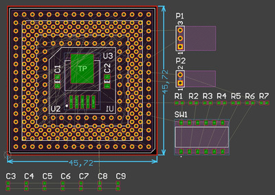
I looked through the wiring of the VRM; it looks correct. On the testbed, I had R7 = 121-ohm, and SW1's resistor at 230-ohm, which yielded Vcc = 3.62 V at 0-ohm load, or 3.65 V at 360 mA - 730 mA loads.
My notes indicate that I went with a 10 uF ceramic cap in the input and a 10 uF tantalum cap on the output. I'm not sure if the load cap needs to be a tantalum, but the MIC29302 datasheet mentions, "Tantalum capacitors are recommended for systems where fast load transient response is important."
Note that TAB is GND according to the Microchip datasheet.
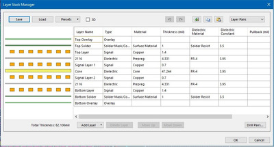
How many layers is the layout?
Are cross-talk, trace capacitance/inductance, reflections, impedence matching, etc. optimised for 66-100 MHz operation?
Plan your life wisely, you'll be dead before you know it.
As short as the traces are going to be, that shouldn't be an issue
I have planned 4 layers (GND plane - Signal layer 1 - VCC plane - Signal layer 2). The VR (TAB) is soldered directly to the GND plane. This also guarantees cooling.
The DIP SW must always be set correctly, never open or several switches on. I don't like that yet...
What do you think of a version like this?
https://www.mouser.de/datasheet/2/972/ss_10_2 … 050-1827383.pdf
No incorrect settings would be possible.
I will make the changes you mentioned soon.
Nothing is optimized yet. A data sheet about the FR-4 material used is also required from the manufacturer for the simulation.
Unfortunately I cannot upload a 3D view as PDF (free 360°), the size exceeds 5MB here at Vogons.
Niemand ist nutzlos, er kann immer noch als schlechtes Beispiel dienen...
Thanks for sending the 3D drawing. I didn't realise Acrobat could display 3D images and allow you to rotate them, view layers, sketches, fill, etc as an option. I'm really outdated.
Yeah, a rotary selector switch would be preferred. Were you looking at model SS-10-16SP-AE from that link you sent? It is a single-pole, 6-throw rotary selector. The issue may be its height of 7 mm. Obviously, we'd want to minimise the gap between the socket and the PCB as much as possible. I'm pretty sure I can get that gap between the sockets and the PCB down to zero, even without solder paste, though I'd like to try some solder paste tests as well. Thus we wouldn't want to source a switch who's height is taller than 4 mm if placing the switch under the PGA-132 pins, which is the preferred location.
For that reason, I have sourced some lower profile rotary switches. Unfortunately, when going shorter, the options for throws is limited. The most common is 4-position and 10-position, with 10 being the most common. 10 positions seems overkill for a VRM on this board, and requires more resistors, but if there's space...?
If going 4-position, we'd do:
3.60 V
3.70 V
3.80 V
3.90 V
If going 6-position:
3.45 V (for running at 50 MHz)
3.60 V
3.70 V
3.80 V
3.90 V
4.00 V
If going 10-position:
3.45 V
3.60 V
3.65 V
3.70 V
3.75 V
3.80 V
3.85 V
3.90 V
3.95 V
4.00 V
For 4-position, this is probably the best bet. It is SMD with leads. 3.75 mm tall and 7 mm x 7 mm footprint.
https://www.digikey.ca/en/products/detail/nid … -7-14TB/2057876
There are even smaller 4 position guys, but the positions aren't numbered and they may be too small, at 2.3 mm tall and 4 mm x 5 mm footprint.
https://www.digikey.ca/en/products/detail/nid … -4-14NTA/948348
For 10-position, there are a lot more options.They are all about 3.75 mm tall and 7 mm x 7 mm. The first one is best because it has leads.
https://www.digikey.ca/en/products/detail/cts … 0AMA10R/4743857
https://www.digikey.ca/en/products/detail/nid … -7010TA/2057866
Or there are 3.9 mm tall units, but they are 10 mm x 10 mm. I think this is too large, but the orange dial looks neat:
https://www.digikey.ca/en/products/detail/nid … /SD-2030/948382
https://www.digikey.ca/en/products/detail/nkk … 10P-W-S/2104083
https://www.digikey.ca/en/products/detail/nkk … FR10P-R/1165796
If there is space, probably go for the first 10-position unit link, otherwise, the first 4-position unit linked above.
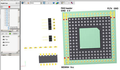
I was also doing some thinking about the headers. Instead of having to increase the PCB real-estate, would it be possible to place the headers on the bottom of the PCB like shown in the mocked up photo below? Note that voltages are deliberately placed inside and GND outside, where possible. I suppose the drawback to putting them on the underside is if there are some components below that hit the headers.
Plan your life wisely, you'll be dead before you know it.
Please note that the 10-position switches are BCD coded. Possible replacement here: https://docs.rs-online.com/80d7/0900766b8152d5b1.pdf
50mV steps would be possible (resistors with footprint 0402). Headers could be tried as SMT.
I'm away over the weekend and unfortunately can't work on the PCB design.
Niemand ist nutzlos, er kann immer noch als schlechtes Beispiel dienen...
Sorry, I missed that some of the switches I sourced were binary coded. The 4-position switch should be good enough. You could select the larger 7x7 mm unit, but if need the space, could go with the 4x5 mm unit.
That Alps switch you referenced, I think will be too large at 12.4 mm x 11.4 mm. Add the lead length, and its footprint is 14mm x 12.4 mm. The usable area on the bottom (and top) of the PCB is about 21mm x 21mm, and you still have caps and resistors to place. Also the Alps switch doesn't appear to have an arrow indicator. I couldn't find a smaller 6+ position SMD switch.
Yes, we could go with surface mounted headers, but with the pushing and pulling of cables, I think the risk of the pad coming off is too high.
I was wondering if it is possible to trim the the PCB footprint down to the area of the white line shown on your photo, that is instead of the red line? I went through several of my 386 boards and was noticing that most manufactuers tend to leave about 4 or 5 mm around the PGA-132 socket before any components turn up. Trimming the PCB to the white line could save about 0.7 mm in either direction.
In most cases, the headers on the bottom wouldn't be used and could even be cut off, desoldered, or never installed if in the way. Thus placing them on the bottom seems like the preferred option since this reduces PCB area. Another idea is to place the headers either under the CPU or inside the PGA-132 foot print, but the user would have to run the wire between the CPU pins which seems tacky.
Plan your life wisely, you'll be dead before you know it.
I just read through entire thread, interested as I didn't see such upgrade adapters before (I only have a 386 for 286 but probably damaged). I'm a bit curious if there is already some real HW after 3,5 years, not just bunch of 3D vis, that would confirm the adapter will work as is without need of extra gates/parts. If I would have that CPU I will make first some dirty and simple PCB to proof it works and then start to playing with extra features like DIP switches and PLLs...
Gigabyte GA-P67-DS3-B3, Core i7-2600K @4,5GHz, 8GB DDR3, 128GB SSD, GTX970(GF7900GT), SB Audigy + YMF724F + DreamBlaster combo + LPC2ISA
The wirewrap model I made showed signs of functionality in the 4-17 MHz range. Just need a trace minimised PCB for testing.
Plan your life wisely, you'll be dead before you know it.
feipoa wrote on 2021-04-04, 01:47:The wirewrap model I made showed signs of functionality in the 4-17 MHz range. Just need a trace minimised PCB for testing.
Nice thread.
So this worked 100% in the end?
The connectivity is all figured?
Well, I think I can also help with the PCB here :p
Let's mod everything! Check my youtube channel:
https://www.youtube.com/channel/UCZ6ULBqIKhxuNslAbqFNJUg
Interested in my devices? Check my store:
https://migronelectronics.bigcartel.com
So you are going to pickup where Aerion left off?
Plan your life wisely, you'll be dead before you know it.
@feipoa:
Sorry that I have not reported here more. Unfortunately I have other PCB projects and too little time.
I will continue this as soon as possible, although I do not own a CPU of this type myself. So I can not test this.
Niemand ist nutzlos, er kann immer noch als schlechtes Beispiel dienen...