VOGONS


First post, by Flakchak

User metadata
Rank Newbie
Rank
Newbie

All,

Happy Father's Day everyone!

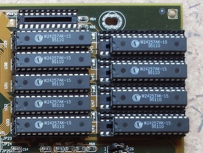
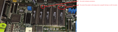
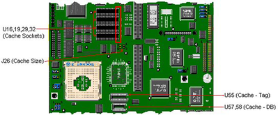
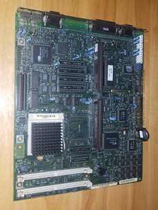
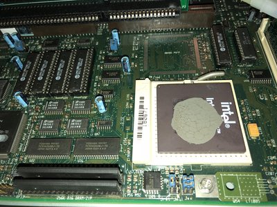
I'm trying my darndest to install cache on my Packard Bell 450 motherboard. I've tried going the 128k and the 512k route.

My jumpers have been in the correct positon, open for none or 128k, and closed for 512k. For the most part when installing the cache, the computer will not post. No booting at all.
Sometimes, it will boot, but whether or not I have "cache enabled" or "cache disabled" in the bios, the info screen during boot will show nothing for L2 cache.

Initially, when I installed the cache chips, the 32k Tag chip (the one on the right) got very hot. So hot that the plastic socket started to melt in the middle.

When I attempted to install the 32k chips in the 4 banks at the left to try a 128k setup, one of the sockets there melted in the middle.

In both instances, there was no further damage to the socket and the chips were able to extracted and reinserted with all points making contact.

Has anyone been successful in putting cache in the PB450 motherboard? Despite the info screen not showing the presence of cache, should I at least reinstall and then run some type of system diagnostic program or speed utility to see if that actually sees the cache installed?

unnamed.jpg
Filename
unnamed.jpg
File size
550.26 KiB
Views
1784 views
File comment
PB450 motherboard
File license
Fair use/fair dealing exception

Searching for a Packard Bell 15" CRT Monitor - 1511SL or 1512SL

Reply 2 of 11, by fitzpatr

User metadata
Rank Member
Rank
Member

You have those chips installed backwards. If something is getting that hot, you should be stopping and questioning everything.

Google pictures of the motherboard, and you'll see that the semi-circle marking on the cache chips should be facing the riser slot.

You should do a good bit more research as far as how these chips should be positioned. they'll need to be rotated 180 degrees, but if you've started the motherboard, it's probable that the chips have been irrevocably damaged. I think that you'll want the 2 rows of pins towards the riser card empty.

View this thread for more information. The post I've linked shows how the cache should be situated.
Cache Upgrade for 486 PB

MT-32 Old, CM-32L, CM-500, SC-55mkII, SC-88Pro, SC-D70, FB-01, MU2000EX
K6-III+/450/GA-5AX/G400 Max/Voodoo2 SLI/CT1750/MPU-401AT/Audigy 2ZS
486 Build

Reply 3 of 11, by Flakchak

User metadata
Rank Newbie
Rank
Newbie
fitzpatr wrote:

I think that you'll want the 2 rows of pins towards the riser card empty.

Thanks, I appreciate the help. To be honest, in my 30 some years of computing, I've never tried to install cache, so even this is new for me. If you look at the link Roman555 provided, it shows how, when, where, etc. the cache should go. Since the text was rightside up, I went with what I saw there and never even thought the chips would be placed the opposite as all the other chips on the board.

If you'll see the portion of your post I quoted, are you talking about the 32kx8 and the 64kx1 right above the processor lever? Why would I want them empty? The cache upgrade page calls for those sockets to be populated by the chips that are there. Should they be rotated 180 degrees as well, just like the four 128kx8 chips that I have inserted incorrectly?

Searching for a Packard Bell 15" CRT Monitor - 1511SL or 1512SL

Reply 4 of 11, by fitzpatr

User metadata
Rank Member
Rank
Member

No problem. 486 and earlier is a very different beast from modern systems. Take your time, and do lots of reading. Most importantly, assume nothing!

All 4 cache chips (U16, U19, U29, U32), the TAG RAM (U55) and the DB RAM (U57/58) are all installed incorrectly.

Cache (SRAM) came in a DIP-28 package, which means that it has 2 rows of 14 pins, totaling 28. This was fine for 32kx8 bit chips (256 kilobit), but when larger capacities arrived, the package needed to be extended so that all of the data could be addressed. This was extended to 2 rows of 16 pins, or DIP-32. If you're using 128kx8 chips (1024 kilobit), it will take up the entire socket, but if you're using 32kx8 chips, it will need to have 2 rows of pins left empty. The semi-circlular notch in the chip indicates orientation. There will always be some kind of mark on the socket or the PCB silkscreening beneath it to indicate which direction the chip must be inserted.

Attachments

  • 0s0a.jpg
    Filename
    0s0a.jpg
    File size
    205.96 KiB
    Views
    1728 views
    File comment
    486 Cache
    File license
    Fair use/fair dealing exception
  • 486 Cache Orientation.png
    Filename
    486 Cache Orientation.png
    File size
    999.44 KiB
    Views
    1729 views
    File comment
    486 Cache SRAM DIP-28 DIP-32 Orientation
    File license
    Fair use/fair dealing exception
  • PB450 empty pins.png
    Filename
    PB450 empty pins.png
    File size
    504.27 KiB
    Views
    1729 views
    File comment
    PB450 Empty Pins Cache
    File license
    Fair use/fair dealing exception

MT-32 Old, CM-32L, CM-500, SC-55mkII, SC-88Pro, SC-D70, FB-01, MU2000EX
K6-III+/450/GA-5AX/G400 Max/Voodoo2 SLI/CT1750/MPU-401AT/Audigy 2ZS
486 Build

Reply 5 of 11, by bjwil1991

User metadata
Rank l33t
Rank
l33t

Hate to bring a thread back to life here, but, on my Packard Bell Pack-Mate 28 Plus (same board revision: PB450), I installed the cache in the correct orientation (watched my dad install L2 cache in our old family computer in 1994), it detected the cache, but, once it gets to the OS, I get all kinds of errors or lock ups when attempting to run the OS, such as MS-DOS 6.22 or Windows 95C.

None of the pins are touching each other, I've straightened them out carefully, tested them one-by-one using my EEPROM programming tool and software on my laptop, which passed with flying colors, thankfully, and still nothing.

I have the following cache chips:

4x Winbond W24257AK-20 28-pin DIP 32K x 8 (256Kb) SRAM
1x WinBond W24257AK-15 28-pin DIP 32K x 8 (256Kb) SRAM TAG
1x AT&T ATT7C187P-15 22-pin DIP 64K x 1 (64KB) - Rebranded Cypress CY7C187-15PC*

* I will test this one when I get home and see if that's the issue, or if there's another issue, such as compatibility issues with Cypress cache chips. A mismatch between the Cypress 22-pin and Winbond 28-pin should work regardless, right? I cannot seem to find a Winbond 22 pin 64K x 1 15ns SRAM DB anywhere online.

Discord: https://discord.gg/U5dJw7x
Systems from the Compaq Portable 1 to Ryzen 9 5950X
Twitch: https://twitch.tv/retropcuser

Reply 6 of 11, by TimWolf

User metadata
Rank Member
Rank
Member

So I'm here trying to find out about cache on this pb450 motherboard I bought on eBay a few years ago. And I'm noticing these melt marks on my cache sockets. I start comparing the manufacturing dates on the chips and then realize I have the exact op board. I guess he sold it when he couldn't figure it out? LoL

Attachments

  • 20220731_164931.jpg
    Filename
    20220731_164931.jpg
    File size
    983.76 KiB
    Views
    781 views
    File license
    Fair use/fair dealing exception

Reply 8 of 11, by TimWolf

User metadata
Rank Member
Rank
Member

So the W241024AK-20 seems to be hard to locate. However the 15ns and 12ns variants are available. Any downside to using the faster cache? The onboard ram has issues but can be disabled. Could any damage beside the OP cache and melting have occurred from thier backwards cache?

Reply 9 of 11, by rasz_pl

User metadata
Rank l33t
Rank
l33t

Yes, I would imagine plugging cache backwards might kill it in a way it temporarily passes VCC to all of its pins first, things on a memory bus might not like that. If you are lucky its only ram and not the chipset/cache controller.

Open Source AT&T Globalyst/NCR/FIC 486-GAC-2 proprietary Cache Module reproduction