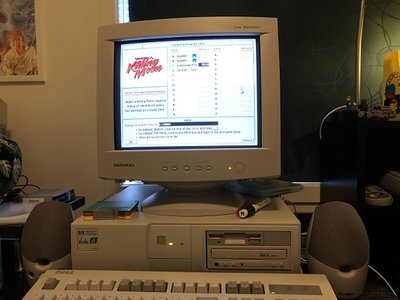
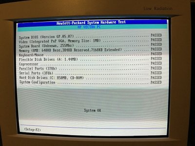
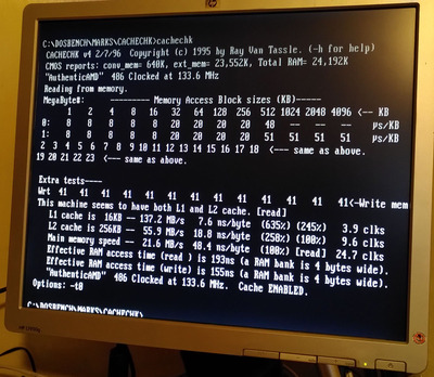
I have a HP Vectra VE 4/100 with a am486 100mhz 8kb L1 WB cache cpu. SIS 496/497 chipset. I have installed the latest HP GP.05.07 bios
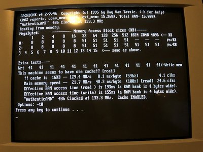
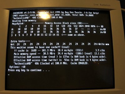
I just got and installed a amd 5x86 cpu With 16kb L1 WB cache. I did not change the 3xmultiplier on the motherboard. The bios detectet it as a 486dx4(wb) 100mhz cpu. I ran some test and i got a nice speed boost from going from 8kb to 16kb L2 cache (5-10%) with the same 3x33mhz clock.
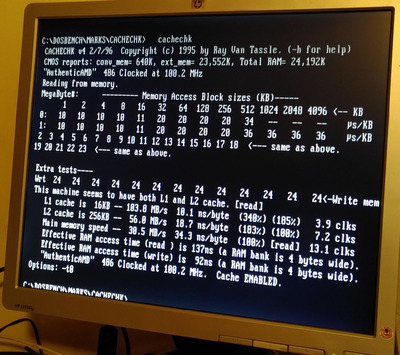
Time for testing 133mhz mode: I changed the jumper on the motherboard to dx2 mode for a 4x multiplier on the cpu. Bios did not detect the cpu correctly (Unknown, 255Mhz). But CPU identification utility and CACHECHK detect the cpu as a 5x86 133mhz 4x33Mhz.
The problem is memory speed is really slow in 133mhz mode. I got lower becnhmark results than before (doom, quake, 3dBench etc)
http://web.inter.nl.net/hcc/J.Steunebrink/amd5x86.htm
"However, a consequence of this incorrect CPU detection can be that the BIOS assumes a higher then actual busspeed. This can result in a degraded performance if the Auto Configuration option in the BIOS Setup is used, because the BIOS programs the chipset with more timing margin than necessary. If this is the case, disable the Auto Configuration feature and set the Cache and DRAM timings to their optimum value."
My bios has memory autodetection, and i cant change the setting. Is there a modified bios i can use? Unlock advanced settings? suggestions?
The motherboard uses a hp/Phoenix bios, can i use one from another sis 496/497 motherboard?
There used to be utilities that could identify hidden bios settings allowing you to (at your own risk) modify the bios manually. Those at Wimsbios May be able to help.
There used to be 5x86 utilities as well though I think they just set cache to wb
My recommendation as silly as it sounds would be to run (for now)
3x40. 3x50 or 4x40 instead and run tests.
I had an old Micronics VLB motherboard that I ran 3x50 for years because the ide was onboard and the video didn’t puke and things worked better setup this way than using the wire trick for 133mhz
There used to be utilities that could identify hidden bios settings allowing you to (at your own risk) modify the bios manually. Those at Wimsbios May be able to help.
Sounds interesting. I should investigate that.
rmay635703 wrote:
My recommendation as silly as it sounds would be to run (for now)
3x40. 3x50 or 4x40 instead and run tests.
I can just use either 33mhz or 25mhz bus speed by using jumpers on the motherboard 🙁
I have this exact same model and also planned to upgrade the CPU to a 5x86 133MHz. Did you succeed in the end?
I was just reading the following part in the technical reference:
DX2/DX4 Type Processors
The CLKMUL pin is controlled by jumper JP16 which is defaulted to x3 mode (DX4). As the DX2 and DX4 are the same component running at a different clock speed, the jumper cannot be left in the DX4 position otherwise the DX2 will also run in x3 clock mode.
The trace on the non-component side of the board which connects pin numbers 2 and 3 of JP16 must be cut. Pin 1 of JP16 can be identified by the square solder pad. JP16 must then be added to the board. The 1-2 connection is the DX2 position and the 2-3 connection is the DX4 position.
Did you cut the trace between pin 2 and 3 as described here?
Edit: I hope it's ok to revive old threads in such a case.
Edit2:
Hmm, the technical reference seems to imply that the pins for JP16 are missing on the board by default, but they're not missing on my board. Since I also just received my 5x86 I decided to give it a go. My setup is slightly different (older BIOS revision and I have the L2 cache module installed) but I get the same issue: Setting the clock multiplier to DX2-mode lowers the memory access speed. I haven't checked the back side of the main board, as it doesn't seem to be that easy to remove.
I guess what I should have said is "Non OEM". Find another motherboard that has similar specs to yours and try swapping in the BIOS.
I can't remember if MR-BIOS exists for the SIS496. I think it may. Sadly, I don't think it's been found yet.
Ah, I see. That makes sense. Maybe if the bios flash chip can be removed / replaced I'd give that a try. I don't want to risk bricking the board. 😀 (I do have a chip programmer though.) How similar do you think these boards need to be to have any chance of success? I guess ideally the BIOS source motherboard should have the same integrated components, number of expansion slots, memory slots? Thinking about this, this HP Vectra has a proprietary L2 cache module specific to a small range of HP Vectra machines. I wonder if that wouldn't already rule out any other BIOS.
The I/O chip is "PC87303VUL Super I/O Sidewinder Lite" made by National Semiconductor Corporation. So far I didn't have much luck finding other board that use this chip + SIS 496/497. Apparently the "Tulip Computers TC40" uses this I/O chip, but it has an intel chipset.
Try to get the old TweakBIOS utility... I think it has support for Sis496 so you can fix the memory timings after booting and regain the performance.
I just tried TweakBIOS v1.53c. Unfortunately it says "Checking for supported BIOS... Not supported." while starting.
It then only shows settings for an AGP device it somehow claims to have found?
Does TweakBIOS actually need the BIOS, or is detecting the BIOS an indirect way of detecting the chipset? I mean, the TweakBIOS website even says "This program can tune probably all computers (running DOS or Windows 95) with one of the following chipsets, CPUs or video cards, regardless of your BIOS".
There doesn't seem to be a way to force the exe to use a certain chipset, but I was wondering, if it only needs the recognise the BIOS to determine the chipset, maybe it would be possible to force it to use the SIS496 configuration? (by hacking the exe I mean)
The problem i have, at least with mine, is that i doesn't have cache... so is a much slower dx2-66.... the cache coast modules are proprietary, and non existing... that's really a shame..
just tried TweakBIOS v1.53c. Unfortunately it says "Checking for supported BIOS... Not supported." while starting.
It then only shows settings for an AGP device it somehow claims to have found?
🤣, maybe it is too buggy. That version does have a file called SIS496.DAT though doesn't it?
Do you have the means to take the BIOS chip out and reflash? ie. to recover from a bricking...? If so then a BIOS patch might be in order.
PG0507US.BIN has a 16 byte header followed by 128KB ROM image. At address $17F6A in the ROM image there is a CPU type detection routine. If the tests fall through then it reaches this code:
1$1802F  B0FF          mov al,0xff
2$18031  2E800EF10018  or byte [cs:0xf1],0x18
0xff is the "unknown" cpu type.
I would try changing 0xff to 0x15 (which is 486DX4 WB) and replace all 6 bytes of the OR instruction with NOPs (0x90)
Thanks for the info on the BIOS. That sounds like it might actually work. However... I inspected the board and I'm not sure yet where the flash bios chip is. In any case it is soldered onto the motherboard, because the only socketed chips on the board are the VGA memory expansion modules. My soldering skills are extremely basic so I'm not confident that I could restore the board if I brick it by flashing it with a non-working BIOS.
I was inspired by your post and by TweakBIOS though. I found the technical manual for the chipset (SiS 85C496/497 Preliminary Rev 3.0 July 1995) and decided to try to program my own tool for modifying the hardware registers of the chipset. Because I thought it would be fun I made the tool in assembly. (and it was 😉) I usually program in C++ and my asm skills are quite basic, but I managed to make something that works. It's here on GitHub. Binary attached to this post. If you have any constructive feedback on my asm soup I'd love to hear it. (I'm pretty sure I could improve the code quite a bit)
The program (which I simply called McSiS496) allows reading and writing from/to the configuration registers in the PCI configuration of the SiS496/497. I didn't implement anything to access/modify registers in "85C497 I/O space (Port 22, 23), or CPU direct I/O space (206)". This does allow modifying DRAM and cache speed/wait state settings etc, just like TweakBIOS. Effectively, you could say I have made a poor man's TweakBIOS. 😜 But it works on this PC!
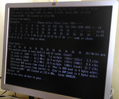
I booted the PC with the CPU in 100MHz mode, recorded the values of registers 40h-43h, which contain the interesting bits (literally). I then set the jumper on the main board to put the CPU in 133MHz mode and after booting used my little program to modify the registers to match what was there previously. Benchmarks in dosbench were much improved after that. I even tried setting the DRAM speed to the 'Fastest' setting (which seems to work fine) and tried 'DRAM Write Cycle Post' (which resulted in a bios error when rebooting).
I'm still testing, but the following has given me the best results so far.
CPU Configuration register 40h:
1mcsis496 b40 0=11 2=010 5=1 6=1
2mcsis496 b40 0=1101011
3
40=11 sets DRAM Speed to Fastest
52=010 sets CPU to Enhanced Am486
65=1 enables CPU Internal Cache Write Back Mode
76=1 enables CPU Burst Write
8
9Register 81h must be updated to match the CPU setting:
10mcsis496 b81 2=010
DRAM Configuration register 41h
1mcsis496 b41 0=1 1=1 2=0 3=1
2mcsis496 b41 0=1011
3
40=1 sets DRAM CAS Precharge Time from 2T to 1T
51=1 sets DRAM Write Cycle CAS# Pulse Width from 2T to 1T
62=0 disables DRAM Write Cycle Post, 0 wait state (enabling this resulted in a bios checksum error when rebooting)
73=1 sets DRAM RAS# to CAS# Delay from 3T to 2T
Cache Configuration registers 42-43h
1mcsis496 w42 9=1 11=1
2
39=1 sets L2 Cache / DRAM Single Read or Burst Read Lead-off Cycle Wait State from 3T to 2T
411=1 sets L2 Cache Single Write/Burst Write Cycle from 3T/2T to 2T/1T