First post, by jammaster
Rank
Newbie
...Between original Intel 486 DX2 and DX2ODPR66 ???
the two are 5V with 8KB of L1, 168Pins, x2 multiplier ... and ?
...Between original Intel 486 DX2 and DX2ODPR66 ???
the two are 5V with 8KB of L1, 168Pins, x2 multiplier ... and ?
Different pinout. That's about it.
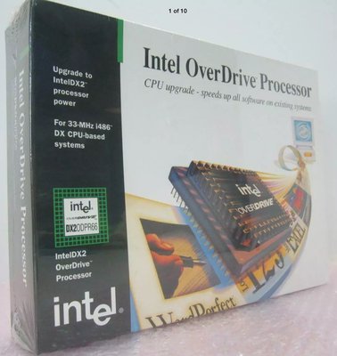
There are two different versions of the DX2 overdrive too. ODP and ODPR. ODP sits in the 487 socket beside the 486SX, but when it is plugged in the 486SX is deactivated. I think these came out before the ZIF sockets were common, and it was designed to make upgrading easier. With the ODPR version, you need to remove the existing 486SX chip and drop the overdrive into the main 486 socket. I think it has a 486SX pinout rather than a 486DX pinout so you don't have to change the jumpers on the motherboard. Internally they're all the same.
"Will the highways on the internets become more few?" -Gee Dubya
V'Ger XT|Upgraded AT|Ultimate 386|Super VL/EISA 486|SMP VL/EISA Pentium
Can’t find the source, but I think ODPRs have write-back cache while regular DX2s had versions with both write-through and write-back.
DX4ODPR100 & 75, sure these chips have WB cache.
But not sure for DX2ODPR66.
(just see the back of the cpu, the die of a WB one is larger than a WT)
DX2ODPR66 seem to be a DX2 badged with an heatsink (!)
To be fair, Socket 2 and 3 can work with both versions.
I must be some kind of standard: the anonymous gangbanger of the 21st century.
ODPR chips are basically the same as the original DX2 and fit into all 486 sockets including the original 168-pin Socket 486. The R stands for replacement so they are direct in-place replacements for SX/DX chips.
ODP chips have one extra pin and can not be installed into the 168-pin Socket 486 sockets, but are instead installed into 169-pin Socket 1 (Overdrive) sockets. As such they are not meant to be direct replacements for Socket 486 CPUs, but they can be installed into any Socket 2 and onwards board and will run as a normal 486DX2 regardless.
For all intents and purposes, they are 100% the same except from 1 extra pin on the ODPR CPUs.
Retronautics: A digital gallery of my retro computers, hardware and projects.
None of the Overdrive chips have write back cache, even as an option. What would be the point? Almost all the older 486 designs did not support write back cache, so it wouldn't work anyway. The only mainstream company that attempted to produce such an upgrade product was Evergreen. It was called "Cacheback" technology, and I don't know that it really worked as advertised. I think a few Japanese upgrades might have had similar designs too. They all required a special software driver for it to "work".
Furthermore, the Intel DX4 overdrives are hardwired to a 3X multiplier. So, if you want 2x50 you need to get yourself a regular DX4 and a 3rd party VRM module.
Also, just for clarification, the 487SX and the ODP chips use identical pinout. You can kind of think of the 487SX as an overdrive without clock doubling, or you can think of the overdrive as a 487SX2.
"Will the highways on the internets become more few?" -Gee Dubya
V'Ger XT|Upgraded AT|Ultimate 386|Super VL/EISA 486|SMP VL/EISA Pentium
wrote:...Between original Intel 486 DX2 and DX2ODPR66 ???
the two are 5V with 8KB of L1, 168Pins, x2 multiplier ... and ?
Some overdrive CPUs are design for computers like the IBM PS/1 which have a additional socket for overdrive CPU’s.
This socket has 1 extra pin which when you plug in the overdrive CPU it disables the onboard CPU so only the overdrive CPU is working. I don’t know what this pin is called technically but I refer to it as PIN number 169
Because that is what the total pin count adds up to as opposed to 168 pins for a standard 486 CPU.
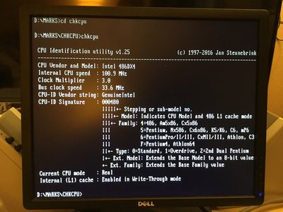
I think most overdrive CPU’s have a built in voltage regulator so you only need to set the CPU bus speed with jumpers on the motherboard to run at 25mhz or 33mhz.
25mhz x 2 = 50mhz.
25mhz x 3 = 75mhz
33mhz x 2 = 66mhz
But most 486 overdrive CPU’s labeled DX2 33 or 66 actually run at 66mhz.
It’s confusing I know, I don’t know why Intel labled the ODP4dx-33 overdrive CPU but it actually runs at 66mhz ?
Where I have a 486sx-33 overdrive CPU that only runs at 33mhz.
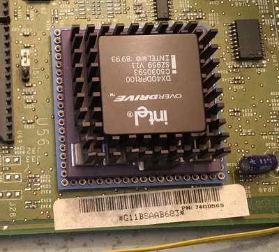
For DX4 Overdrive CPU
33mhz x 3 = 100mhz
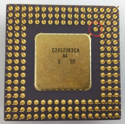
Is that last image of an ODP chip? My ODPRs definitely don't have 169 pins.
"Will the highways on the internets become more few?" -Gee Dubya
V'Ger XT|Upgraded AT|Ultimate 386|Super VL/EISA 486|SMP VL/EISA Pentium
wrote:Is that last image of an ODP chip? My ODPRs definitely don't have 169 pins.
ODPR is supposed to Replace existing CPU, thus it fits in the normal socket. The 169 pin only fits the OverDrive socket AFAIK, which will make it an ODP.
Please use the "quote" option if asking questions to what I write - it will really up the chances of me noticing 😀
There are different versions (steppings) of the DX2 and the overdrive. That’s what creates the difference.
The only obvious difference (apart from the integrated heatsink) between any DX2 and DX2ODPR is absence of the boundary scan feature on the overdrive (apart from certain sample chips).
wrote:There are different versions (steppings) of the DX2 and the overdrive. That’s what creates the difference.
The only obvious difference (apart from the integrated heatsink) between any DX2 and DX2ODPR is absence of the boundary scan feature on the overdrive (apart from certain sample chips).
This is interesting, I never knew this. Are there any real world implications of this ommission?
Retronautics: A digital gallery of my retro computers, hardware and projects.
wrote:None of the Overdrive chips have write back cache, even as an option.
From: https://en.wikipedia.org/wiki/Intel_80486_OverDrive
Intel's i486 OverDrive processors are a category of various Intel 80486s that were produced with the designated purpose of being used to upgrade personal computers. The OverDrives typically possessed qualities different from 'standard' i486s with the same speed steppings. Those included built-in voltage regulators, different pin-outs, write-back cache instead of write-through cache, built-in heatsinks, and fanless operation — features that made them more able to work where an ordinary edition of a particular model would not.
They actually had WB cache before "normal" CPUs had it.
Conceptually, the OverDrive was an upgrade chip, marketed at end-users.
These chips would contain a glued-on heatsink, and would be drop-in replacements for any compatible machine (without having to worry about adding/changing fans, PSUs or anything).
The 'vanilla' DX2 was only aimed at new systems, and the system builder would have to take care of the proper cooling solution and power supply.
It might be that the OverDrive chips were 'cherry picked' to make sure they had the lowest power consumption and heat dissipation, given their intended use.
I sincerely doubt binning for thermals was even a thing at the time..
Retronautics: A digital gallery of my retro computers, hardware and projects.
wrote:I sincerely doubt binning for thermals was even a thing at the time..
Sure it was. Why else did you think Intel sold multiple speed grades of their CPUs at the same time?
Heck, the whole 486DX/SX thing is a result of binning: working FPUs or not.
wrote:wrote:I sincerely doubt binning for thermals was even a thing at the time..
Sure it was. Why else did you think Intel sold multiple speed grades of their CPUs at the same time?
Heck, the whole 486DX/SX thing is a result of binning: working FPUs or not.
They binned for operating frequency of course, but not for thermals or efficiency - that's what I was saying.
Retronautics: A digital gallery of my retro computers, hardware and projects.
wrote:Wasn't that only the case in the early days of the 486SX?
Yea, eventually they physically removed the FPU, so it actually was a different, smaller/cheaper die (I presume the yields for 486DX were high enough that this was now a better economic proposition).