VOGONS


First post, by mkarcher

User metadata
Rank l33t
Rank
l33t

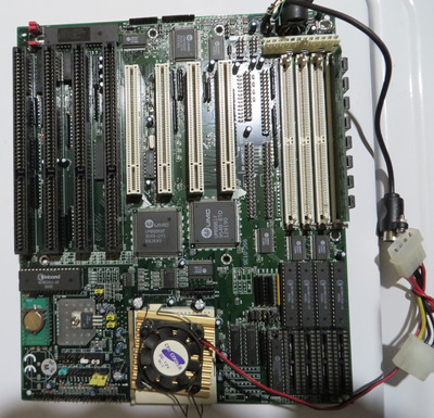
I successfully added PS/2 support to Disruptor's Shuttle HOT433 (rev 1, 2 or 3) mainboard (using an external KBC). This post is a detailed explanation on what needs to be modified on the board to switch it to external keyboard controller support, and suggests a BIOS image that can be used as base.

About the keyboard options of the UM8886
Integrated keyboard port
The UM8886 south bridge (commonly paired with the UM8881 north bridge on 486 boards) has an integrated keyboard controller, including PS/2 mouse support. It uses mulifunction pins for the keyboard and mouse interface. In this post, I am not going to use the integrated PS/2 mouse support of the UM8886, because the traces needed for that are not available on the Shuttle HOT433, and modding that board for support of the integrated PS/2 mouse support would be a tedious and delicate task.

The keyboard interface part of the integrated keyboard controller is combined with control pins for the external keyboard controller. The following pins of the UM8886 are relevant for the keyboard interface (integrated KBC) or keyboard controller interface (external KBC), the color code is the color I use in the images to highlight traces connected to that pin. No worries for color-blind people, I will also explain the connections in readable text:

Pin nr    IntKBC        ExtKBC                                      Color code
55 Keylock Keyboard controller clock dark brown
56 Kbd Data CPU reset from keyboard controller green
57 Kbd Clock A20 gate from keyboard controller yellow
58 /ROMCS * /KBDCS in both modes, also configuration strap hot pink

As you see, pins 55 to 57 change to completely different functions when you switch between internal and external keyboard controller mode. Not even the direction of those pins stays the same. In internal KBC mode, pin 55 is an input pin (5V = keyboard unlocked, 0V = keyboard locked), whereas pin 56 and 57 are high-drive open-collector bidirectional pins that can be directly connected on the DIN or PS/2 connector without any buffer chip. In external KBC mode, pin 55 is an output pin, carrying the processor clock for the keyboard controller (around 8MHz), whereas pins 56 and 57 get input pins for system control signals that originate from the keyboard controller.

Pin 58 does not change its function, but still a very important dual-purpose pin. It's primary purpose is to be a chip select signal for both the ROM BIOS chip as well as the keyboard controller. UMC pulled a clever trick here, because both the keyboard controller and the ROM BIOS only actually do something if their chip select signal is combined with a second signal. This second signal is "memory read" or "memory write" for the BIOS chip (obviously, write is only useful on flash parts), whereas the second signal is "I/O read" or "I/O write" for the keyboard controller. So the keyboard controller and the ROM BIOS chip can always be selected at the same time, but the ROM chip only responds on memory cycles, and the keyboard controller only responds on I/O cycles. The secondary function of Pin 58 is the most important function of this whole post: It's a configuration strap that tells the UM8886 whether the internal keyboard controller is to be enabled or disabled. If this pin is pulled high at power-up, the internal keyboard controller is enabled, and Pins 55-57 have the function listed in the second column of the table above. If pn 58 is pulled low at power-up, the internal keyboard controller is disabled, and Pins 55-57 have the function listed in the third column of the table. I wasted some time trying to find a PCI configuration space bit to toggle between internal and external KBC mode - just to find out that there seems to be none.

Integrated mouse port
While this post is not about the integrated PS/2 interface, I also reverse engineered something about the PS/2 port. I will write down the results in this paragraph, but you can skip until the next heading for the main point of this post.

The PS/2 mouse interface is multiplexed on pins used for the "ISA unlatched high address lines". These address lines are introduced with the 16-bit ISA extension of the IBM AT and present the address for the next cycle quite early (possibly even when the previous cycle is just about to be finished), and are not necessarily valid over the whole bus cycle. The primary purpose of LA17-LA19 is allowing 16-bit ISA plugin cards to signal their capability of handling a 16-bit cycle. This is used by 16-bit VGA cards for video memory access if they detect LA17-LA19 having the pattern 1,0,1 (which translates to the address range A000:0 to B000:FFFF). To allow zero-waitstate 16 bit memory writes, the MEMCS16 and 0WS pins need to be driven before the old-fashioned SA17-SA19 lines are guaranteed to be valid. The high address lines (to extend ISA from 1MB to 16MB address range) are also only presented as unlatched lines LA20 to LA23, and they need to be decoded by cards responding to past-1MB writes. The following pins change their function depending on enabling the internal PS/2 port:

Pin nr   Mouse port on    Mouse port off
198 unknown LA19
199 Mouse Data LA18
200 Mouse Clock LA17

On the Biostar 8433UUD board, which uses the integrated mouse port of the UM8886 south bridge, the connections of pin 198 to 200 can be reassigned to either the ISA LAx pins or the mouse port pins by moving a soldered resistor network (of the 4*0Ohm type). The specific 8433UUD I have at hand obviously has the resistor network soldered at the position that connects these pins to the PS/2 mouse port. The ISA pins LA17 to LA19 are driven from SA17 to SA19 instead. My guess it that this reduces ISA compatibility with 16-bit cards, because you can not drive LA17-LA19 and SA17-SA19 from the same pin without violating some ISA timing specification, but I did not yet get around to do thorough ISA tests (like testing 0WS ET4000 ISA graphics cards) on the UMC board.

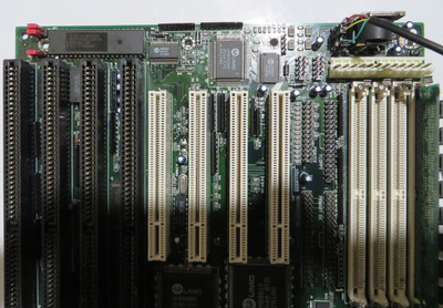
Analysis of the PCB traces on the HOT433
Pinout of the sockets / the mouse pin header
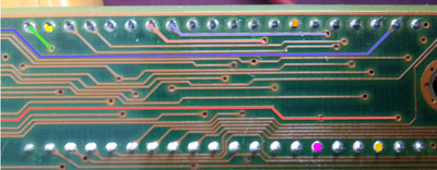
As feipoa already noticed, the assignment of PS/2 mouse port pins to the UMC south bridge is "weird". This is a side effect of a strange choice about what 0-ohm jumper links are configured on the board as sold. I am going to show photos of relevant parts of the board (some from the back, just to show the traces; some from the front to show SMD components) to explain what needs to be modified. The relevant traces are color-coded, an I am also explaining them in plain text for color-blind readers.

Let's start with the pins at the keyboard and mouse ports. The pinout of those ports are well-known, so identifying the traces is straight-forward. I use the following color-code:

Keyboard Clock    saturated red
Keyboard Data light red
Mouse Clock saturated blue
Mouse Data light blue
+5V white
GND black
AtTheSockets.jpg
Filename
AtTheSockets.jpg
File size
109.52 KiB
Views
2643 views
File license
CC-BY-4.0

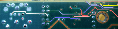
This part shows the traces from the keyboard port and the 10-pin header for the mouse (pin 1 is at the top right corner, pin 2 at the top left corner, pin 10 at the lower left corner) going towards the keyboard controller. It connects the standard pins from the DIN socket (and the soldering pads for the alternate option for a PS/2 keybord socket at the same place) to some vias that connect to very import zero-ohm resistors shown in the next picture. The pinout of the 10-pin mouse header ist like this:

  • Pin 2: GND
  • Pin 3: Mouse data
  • Pin 5: +5V
  • Pin 10: Mouse clock

Except for the red and blue wires from the port, the top right corner also shows a yellow and a green trace. These traces are directly connected to the chipset pins listed in the first table.

pull-up and "configuration" resistors between the sockets and the super I/O chip
On the other side at the board, you find the following layout:

Between.jpg
Filename
Between.jpg
File size
138.47 KiB
Views
2642 views
File license
CC-BY-4.0

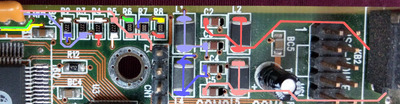
This picture shows the L/C filters for the keyboard and mouse clock and data lines (where no attempt is mode to use different colors for the "external" and "internal" side of the L/C filters). This picture also shows the pull-up resistors for the clock and data lines. Keyboard clock is filtered by C2/L2 and pulled up by R4, keyboard data is filtered by C5/L5 and pulled up by R5, mouse clock is filtered by C4/L4 and pulled up by R2, finally mouse data is filtered by C3/L1 and pulled up by R3. Notice the white color-code (for +5V) on the opposite end of the pull-up resistors.

If no external keyboard controller is present, keyboard clock and keyboard data need to be directly connected to the yellow-coded and green-coded line from the chipset. This is achieved by R6 and R8. If you want to use an external keyboard controller, remove R6 and R8. R7 is a kludge for an external AT keyboard controller without PS/2 mouse support. An AT keyboard controller has the keyboard data line connected to Pin 39, whereas a PS/2 keyboard controller has the mouse clock at the same pin. So the purpose of R7 is to connect the keyboard data line (light red) to the correct pin of an AT keyboard controller. As the goal is to install a PS/2 keyboard controller with mouse support, remove R7.

Interesting pins at the keyboard controller
Pins that are relevant to understand the modification are (at the keyboard controller):

AtTheKBC.jpg
Filename
AtTheKBC.jpg
File size
132.93 KiB
Views
2610 views
File license
CC-BY-4.0
  • Pin 1 is keyboard clock input to the KBC, color coded saturated red
  • Pin 3 is controller clock input (~8MHz) to the KBC, color coded light brown
  • Pin 6 is chips select to the KBC, color coded hot pink (shared with BIOS chip select, as explained above)
  • Pin 21 is CPU reset output from the KBC, color coded green
  • Pin 22 is A20 gate output from the KBC, color coded yellow
  • Pin 27 is keyboard data input to the (PS/2) KBC, color coded light red
  • Pin 28 is mouse data input to the (PS/2) KBC, color coded light blue
  • Pin 34 is keylock input to the KBC, color coded orange
  • Pin 39 is mouse clock input to the (PS/2) KBC, color coded saturated blue (an AT KBC has keyboard data on this pin; if you use an AT KBC, you need R7 to bridge keyboard data input into this pin.

Configuration area next to the 7406 socket
The 7406 socket needs to be fitted with an 7406. The 8042 keyboard controller chip is not able to drive a long keyboard cable, so it needs an external ampliefer. The most simple kind of digital amplifier is an inverter. The 7404, 7405 and 7406 all are inverter chips (containing 6 inverters), but only the 7405 and the 7406 are so-called open-collector inverters (they pull the signal low if needs to be low, but they don't do anything if the signal should be high). The keyboard interface relies on this behaviour to enable bidirectional communication. If neither the keyboard nor the 7406 on the mainboard pull the signal low, it is pulled high by the corrensponding pullup resistor on the mainboard. If either device pulls the signal low, it pulls much stronger than the pull-up resistor, so the signal appears low. The 7406 is a much stronger inverter than the 7405 (it can pull down more current, so it can (dis)charge the keyboard cable faster), so the keyboard interface uses the 7406. Only 4 of the 6 inverters are used (two for the mouse interface, two for the keyboard interface), in case of the HOT433, the inverters at pin 1 and 2, at pin 3 and 4, at pin 5 and 6, as well as the inverter at pin 9 and 8 are used. The inverters at pins 11 and 10 as well pins 13 and 12 are unused. The traces from the keyboard controller output to the 7406 sockets are not shown in my pictures, because they follow the standard PS/2 keyboard controller layout and don't help in understanding how this specific board works.

Next to the 7406 sockets, you find the following components:

NextTo7406.jpg
Filename
NextTo7406.jpg
File size
118.07 KiB
Views
2642 views
File license
CC-BY-4.0

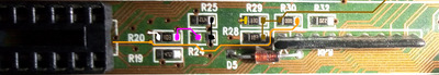
In this picture, the following connections are visible:

  • Keylock (connected to the keylock pin at the front panel connectors and pin 34 of the keyboard controller, color coded orange, is connected to the right side of R30.
  • Keyboard controller clock (connected to pin 3 of the keyboard controller, color coded light brown) is connected to the left side of R29
  • The multi-function pin for keylock or keyboard controller clock from the chipset (color coded dark brown), is connected to the right side of R29 and the left side of R30. The function of R29 (33 Ohms) is to absorb reflections of the the clock signal that might arise at the keyboard controller or its socket. This is called "series termination".
  • Keyboard Controller/ROM chip select (color coded hot pink) is connected to the right pad of R20 (10 kOhm) and to the left pad of R24 (inentionally absent)
  • the left pad of R20 is connected to +5V (color coded white)
  • the right pad of R24 is connected to GND (color coded black)

If an external keyboard controller is to be used, the chipset does no longer need to receive the keylock signal, but it starts outputting the clock signal for the keyboard controller on the corresponding multifunction pin. Thus the dark brown line now is keyboard controller clock and needs to be disconnected from the keylock signal. Remove R30. Also, as explained in the introduction, the UM8886 needs to know that an external keyboard controller is present, so the keyboard controller/ROM chip select signal no longer needs to be pulled up (through R20), but it needs to be pulled down (through R24). So remove R20 and place the resistor on the R24 pads instead.

BIOS
You need a BIOS with enabled PS/2 mouse support. I recommend using the bios with the identifier string 2A4X5H21, as posted in this thread Newer AWARD Bios for HOT-433?, as it seems to be based on a quite recent revision of the Award 4.51 core. This BIOS has PS/2 mouse support disabled through a configuration bit which can be changed by MODBIN on the "installed options" page. I did so to obtain this image:

Filename
2A4X5H21+Mouse.zip
File size
84.04 KiB
Downloads
108 downloads
File license
Fair use/fair dealing exception

You need to flash this BIOS and enable "PS/2 mouse function" in the advanced BIOS setup options page to obtain a working PS/2 port.

Keyboard controller
You need (obviously) a PS/2 compatible keyboard controller. In this case, it's a MEGAKEY taken from a dead donor board. These 8042 controllers contain an internal oscillator that outputs pulses on pin 2, and expect to excite a crystal in resonance that is connected between pins 2 and 3. The signal that comes back on pin 3 is used as system clock and as reference to create excitation pulses on pin 2 at the right frequency. If you want to clock the keyboard controller from an external clock (as these mainboards do), you just feed the clock into pin 3, while pin 2 should be left alone. The shuttle HOT-433 seems to have a supply rail connected to that pin right at the socket, so the excitation pulse output of the keyboard controller is shorted to ground (or +5V). This is not nice towards the keyboard controller and should be avoided (but it would most likely work anyway). I dealt with this problem by bending pin 2 upwards, so it stays next to the socket instead of being inserted.

Summary
So, in a TL;DR manner: To enable the PS/2 mouse port on your HOT433 boards, do the following tasks:

  • Remove R6-R8 (0-Ohm resistors next to the PS/2 mouse pin header)
  • Remove R30 (0-Ohm resistor near the 7406 socket)
  • Move the 10kOhm resistor (marking code "103") from R20 to R24. Originally, R24 is absent, after the mod, R20 is absent.
  • Plug a 7406 chip into the empty socket marked 7406 (between the ISA slots)
  • Plug a PS/2 compatible keyboard controller into the empty socket marked 8042. Preferably avoid contacting pin 2 by pending this pin out of the socket.
  • Flash a BIOS with PS/2 mouse support enabled, for example the one included in this post

EDIT: Added the story about bending the clock oscillator output pin.

To undo the modification, revert all the changes, except you don't have to re-install R7.

Last edited by mkarcher on 2020-06-21, 21:07. Edited 2 times in total.

Reply 1 of 25, by mkarcher

User metadata
Rank l33t
Rank
l33t

By the way, I recently ordered some UV-erasable 8042 chips (i.e. 8742 chips) that can be used as keyboard controllers. Does anyone know a (preferably legal) source for a PS/2 compatible firmware image for them? I just assumed the open-source community already had developed suitable firmware, but my Google-Fu is not sufficient to find such a project.

Reply 2 of 25, by darry

User metadata
Rank l33t++
Rank
l33t++

This is neat . Great job on project and documentation .

I would guess that a good source for pre-programmed keyboard controller chips would be dead boards, damaged beyond repair by leaky batteries .

Reply 4 of 25, by Tiido

User metadata
Rank l33t
Rank
l33t

I'm wondering, do you have any documentation about these chipsets ? You mention strap pins etc.

Nice work ~

T-04YBSC, a new YMF71x based sound card & Official VOGONS thread about it
Newly made 4MB 60ns 30pin SIMMs ~
mida sa loed ? nagunii aru ei saa 😜

Reply 5 of 25, by Disruptor

User metadata
Rank Oldbie
Rank
Oldbie

There was no documentation.
However, to compare wiring traces he used a Gigabyte GA-486IM and a Biostar MB-8433UUD. Both use the same chipset but in different revisions. The Gigabyte has an external KBC but no mouse port. The Biostar has an internal KBC with working mouse port.
And, yes, he reads assembler code (BIOS) like a book.
A multimeter is nice, but an oscilloscope revealed another secret.

Reply 6 of 25, by mkarcher

User metadata
Rank l33t
Rank
l33t
Tiido wrote on 2020-06-22, 21:43:

I'm wondering, do you have any documentation about these chipsets ? You mention strap pins etc.

No, I do not have any documentation. There is a thread here on VOGONs requesting documentation for UMC chipsets in UMC8881/8886 Datasheet. This thread contains a schematic for a pentium-based laptop that still uses the UM8886 south bridge. This schematic has pin numbers and pin names included, but it seems the labels of the multi-function pins are not exhaustive. Yet it is this schematic that pointed me to the chip-select being dual-purpose for both the BIOS ROM and the Keyboard controller.

I obtained all the information I posted in the original post from reverse engineering and comparing three different UM8881/UM8886 based boards: The Shuttle HOT433 (internal KBC, keyboard only), the Gigabyte GA486IM (with dedicated keyboard-only KBC) and the Biostar 8433UUD (internal KBC, keyboard + mouse). Finding the configuration strap pin to enable/disable KBC was partly being lucky. I knew from reverse engineering (i.e. buzzing out connections on the HOT433) that there is a multi-function pin that shares keylock and keyboard controller clock. As long as R30 was installed on the HOT board, I could easily pick up the signal from that pin at the keylock connector with my oscilloscope. I knew that I got to see a clock signal there if the UM8886 is sucessfully switched to external keyboard controller mode. I tried messing around with toggling all configuration bits in the PCI configuration space of the south bridge, but while I managed to make the southbridge configuration space disappear from the PCI bus (at least at address 12.0) and I managed to crash the system by blindly toggling bits, I did not manage to find a bit that enabled keyboard controller clock output.

I then compared the BIOS image from a Shuttle HOT433 rev 4 (for which I mistakenly believed it came with an external KBC) to the BIOS image for a Shuttle HOT 433 rev 1-3, and did not find any initialization differences between the different board revisions until the keyboard controller was initialized. Despite the wrong assumption, I came to the correct conclusion that there is no software configuration for the keyboard controller, but it has to be a hardware strap. Now I wondered what pin the strap might be on. As keyboard clock/keyboard data are implemented using open collector outputs with a weak pull-up, these pins are not suited to be strap pins. The keylock/kbc clock pin can not be a strap, because in the case of internal KBC, the pin might either be high or low at power-on depending on the keylock state. So the strap has to be on a different pin. I then wondered wheter there are further pins at the UM8886 south bridge that interact with the keyboard controller, and luckily I thought about "hey, there needs to be a chip select output for the external KBC. There seems to be no decoder for Port 60/64 in dedicated logic or the super I/O chip, so that decoder needs to be in the south bridge". And it was easy to buzz out that this pin is right next to the keyboard interface / keyboard controller interface pins. Also, a chip select output (which is permanently driven by the UM8886) is a sensible choice for a strap input. I found out that the HOT433 has a 10K pullup on this pin, the Biostar 8433UUD has a 4.7K pullup on this pin while the GA486IM has a 1k pulldown on this pin. Furthermore, I identified that the HOT433 board obviously is designed in a way that pulling up or pulling down that line is a variation to be chosen by component placement, so it seemed quite plausible to be on the right track.

I felt lucky, connected the scope probe to keylock, and identified a 1k pulldown resistor on DRQ1. So I shorted the keyboard controller chip select signal (with its 10K pullup) to DRQ1 (with its 1K pulldown) to override the pullup, and on power-on, I got a 5V squarewave output on the keylock input pin header of the mainboard. It felt like party time, and the remaining steps to modify the board were obvious.

(edit: just minor editorial changes)

Reply 7 of 25, by Tiido

User metadata
Rank l33t
Rank
l33t

That's a really great effort, very awesome ~

I'm hoping to get a UMC8886/1 based board soon, I will come back to this thread at some point then.

T-04YBSC, a new YMF71x based sound card & Official VOGONS thread about it
Newly made 4MB 60ns 30pin SIMMs ~
mida sa loed ? nagunii aru ei saa 😜

Reply 9 of 25, by Chadti99

User metadata
Rank Oldbie
Rank
Oldbie
citronalco wrote on 2021-11-25, 17:37:

This really works!
Thank you for your work, and for the detailed instructions.
I simply followed them step by step, was pretty easy!

Hi citronalco, did you pull the keyboard controller from another board or source one online? Trying to find a source myself.

Fantastic write-up @mkarcher!

Reply 10 of 25, by citronalco

User metadata
Rank Newbie
Rank
Newbie

Pulled it from an old board.

Have to admit that while PS2 keyboard and mouse connectors work completely flawless with a real keyboard and mouse, they do not with my KVM (Belkin OmniView Pro 😎: I get lost keypresses, double key presses, and the mouse does not work at all.

Reply 11 of 25, by mockingbird

User metadata
Rank Oldbie
Rank
Oldbie
citronalco wrote on 2022-09-29, 22:13:

Pulled it from an old board.

Have to admit that while PS2 keyboard and mouse connectors work completely flawless with a real keyboard and mouse, they do not with my KVM (Belkin OmniView Pro 😎: I get lost keypresses, double key presses, and the mouse does not work at all.

I will test this mod in the near future with my Avocent KVM and report back.

mslrlv.png
(Decommissioned:)
7ivtic.png

Reply 12 of 25, by mockingbird

User metadata
Rank Oldbie
Rank
Oldbie

Fantastic mod, thanks 😀

I did not socket the KBC, for fear of the added height interfering with ISA cards. I bent pin 2 out, and it's touching the back of the ISA slot.

The PS/2 worked perfectly fine with my Avocent KVM (tested with Microsoft Mouse driver and Monkey Island). All I can suggest is to try a different KBC. I used a Mega-KB revision F. I must have pulled this thing off of something decades ago. I never thought I would end up using it. Just goes to show you.

IMG_1843.JPG
Filename
IMG_1843.JPG
File size
1.43 MiB
Views
1518 views
File license
Public domain
IMG_1844.JPG
Filename
IMG_1844.JPG
File size
1.41 MiB
Views
1518 views
File license
Public domain

mslrlv.png
(Decommissioned:)
7ivtic.png

Reply 13 of 25, by feipoa

User metadata
Rank l33t++
Rank
l33t++

@mkarcher, do you remember if the BIOS presented here contains the IRQ routing table fixes and LatePCI noted by Disruptor from this thread? Thanks!
My 486 UMC8886/8881 Project (Version 2.0)

Plan your life wisely, you'll be dead before you know it.

Reply 14 of 25, by mkarcher

User metadata
Rank l33t
Rank
l33t
feipoa wrote on 2023-02-19, 09:31:

@mkarcher, do you remember if the BIOS presented here contains the IRQ routing table fixes and LatePCI noted by Disruptor from this thread? Thanks!
My 486 UMC8886/8881 Project (Version 2.0)

This BIOS does contain the correct IRQ routing table, because it is an actual HOT-433 BIOS. We only got IRQ routing issues when we cross-flashed a BIOS from a GA-486AM or a Biostar MB8433-UUD. This BIOS does not yet contain the "LatePCI" stuff. That patch has been performed later, and is posted in Matrox G450 (with DVI outout) working on a HOT433 main board (UMC 8881) . This patch is not required for any kind of PCI IDE controller, and the the LPCI40.BIN variant may actively prevent POSTing at 40MHz FSB if you want/need PCI@20 because some card can't handle PCI@40. Please use the LPCI40.BIN only if you need PCI@40 during the POST before option ROMs are initialized. The only use case I know as of now is the Matrox G450 PCI, which can't be properly set up at 20MHz PCI clock. Other PCI/AGP-bridged based graphics cards might have the same issue. You are likely fine to use LPCI33.BIN in any practically relevant scenario. The main difference between the mouse-enabled BIOS from this thread and LPCI33 is that with LPCI33 PCI resource assignment happens at PCI=FSB for FSB frequencies up to 33MHz, and it only performs resource assignment at PCI=FSB/2 for FSB40 and higher. The original mouse-enabled BIOS performs PCI resource assignment at PCI=FSB/2 at every FSB clock. Either BIOS switches to PCI=FSB during the POST if FSB=33MHtz, and only applies the setting from the CMOS after FDD and HDD has been seeked/initialized. To run a 33MHz FSB system at 16.7MHz PCI even during POST, you would need yet another kind of modified BIOS.

Reply 15 of 25, by feipoa

User metadata
Rank l33t++
Rank
l33t++

Thanks for the explanation. I wasn't sure if 2A4X5H21 was a BIOS specific to the HOT-433 or not. I was under the impression it wasn't when I read Disruptor's thread. However, in looking deeper through my archives, it appears to be from esupport.com for HOT-433.

When I free up some other projects, I'm looking forward to doing this PS/2 mod. Have you been able to workout the PS/2 issues with the HOT-433 v4 board?

I will probably hold off on testing the G450 with the Shuttle HOT-433 until I do the PS/2 mod. However, if I recall right, I had trouble getting D3D and OpenGL working w/G450+486, so interest might be limited unless paired with a Voodoo2.

Plan your life wisely, you'll be dead before you know it.

Reply 16 of 25, by mkarcher

User metadata
Rank l33t
Rank
l33t
feipoa wrote on 2023-02-19, 18:52:

When I free up some other projects, I'm looking forward to doing this PS/2 mod. Have you been able to workout the PS/2 issues with the HOT-433 v4 board?

Neither me nor Disruptor owns a HOT-433 v4, so I didn't investigate it. This thread describes the technical details about all the signals on the v1 to v3, and I just checked a photo of the v4 on the retro web. It seems the keyboard controller stuff is very similar. Possibly the unpopulated SO14 spot below the unpopulated keyboard controller socket is an alternate position for the 7406 that still has an unpopulated DIP14 spot next to the keyboard controller. There is one unpopulated SMD resistor position next to the DIP spot marked 7406, which likely corresponds to the R24 position on the v1 to v3 boards. So I encourage you to try to reproduce the measurements I posted in the original post on your v4 board.

feipoa wrote on 2023-02-19, 18:52:

I will probably hold off on testing the G450 with the Shuttle HOT-433 until I do the PS/2 mod. However, if I recall right, I had trouble getting D3D and OpenGL working w/G450+486, so interest might be limited unless paired with a Voodoo2.

If I remember correctly, 3DMark 99 worked out-of-the-box with the G450 after installing recent drivers. There is a general issue with the OpenGL screensavers in Windows 2000 - they implement a bad algorithm to choose the PixelFormat before calling wglCreateContext, resulting in a software rendering context instead of an hardware accelerated context if the graphics cards supplies a full "installable client driver" to implement OpenGL instead of a "mini client driver" that relies on a hardware-independent high-level OpenGL driver. The Matrox G450 drivers contain a full OpenGL driver. I have a patched ssmaze.scr as proof-of-concept, but didn't post about that patch on VOGONS yet.

Reply 17 of 25, by feipoa

User metadata
Rank l33t++
Rank
l33t++

The HOT-433 v4 uses the UM8886BF, which should have built-in PS/2 mouse support. My [eventual] intention for the v4 board was to get it working with PS/2 thru the chipset.

On Disruptor's thread, I noticed he didn't need to mod the Dallas RTC. Can I confirm that all I need to do is add a CR2032 battery holder and this is sufficient for time keeping and CMOS settings?

mkarcher wrote on 2023-02-19, 19:53:

If I remember correctly, 3DMark 99 worked out-of-the-box with the G450 after installing recent drivers.

I think 3DMark99Max is D3D only. Did you try any D3D games or OGL games? EDIT: if yes, in which OSes and with which DirectX versions?

mkarcher wrote on 2023-02-19, 19:53:

There is a general issue with the OpenGL screensavers in Windows 2000 - they implement a bad algorithm to choose the PixelFormat before calling wglCreateContext, resulting in a software rendering context instead of an hardware accelerated context if the graphics cards supplies a full "installable client driver" to implement OpenGL instead of a "mini client driver" that relies on a hardware-independent high-level OpenGL driver. The Matrox G450 drivers contain a full OpenGL driver. I have a patched ssmaze.scr as proof-of-concept, but didn't post about that patch on VOGONS yet.

Interesting. Is this only an issue with some graphics cards, or all? Luckily, I don't think many people are using W2K with their 486's. I don't recall for certain, but I think my G450 card is in my dual socket 5 system with P233MMX chips.

Plan your life wisely, you'll be dead before you know it.

Reply 18 of 25, by mkarcher

User metadata
Rank l33t
Rank
l33t
feipoa wrote on 2023-02-19, 23:34:

The HOT-433 v4 uses the UM8886BF, which should have built-in PS/2 mouse support. My [eventual] intention for the v4 board was to get it working with PS/2 thru the chipset.

OK, I understand. You are on your own then. I have no idea how to configure the built-in PS/2 mouse support on the UM8886BF. As I observed on the Biostar board, the ISA LAxx pins are multiplexed with the PS/2 mouse pins, and there needs to be some way to strap the UM8886BF into either mode.

feipoa wrote on 2023-02-19, 23:34:

On Disruptor's thread, I noticed he didn't need to mod the Dallas RTC. Can I confirm that all I need to do is add a CR2032 battery holder and this is sufficient for time keeping and CMOS settings?

That one is sneaky. The Dallas chip is modded, but you don't see it. As you likely know, the Dallas modules are Dallas chips with some pins bent upwards and the battery and quartz crystal mounted to them, before being potted into that bulky case. On Disruptors HOT-433, the Dallas module has been dremelled at the two pins leading to the battery (you should be able to see it in the first picture in My 486 UMC8886/8881 Project (Version 2.0)). The negative lead of the battery is internally connected to GND anyways, so that one was pointless. The board contains a trace from the CR2032 holder to the positive battery pin for the Dallas chip variant without the included battery. We soldered a wire through the board to the Dallas pin (after making sure the internal battery connection is completely milled away), to connect it to the battery holder. So it's like the classic Dallas mod, but putting the holder onto the board instead of the chip.

feipoa wrote on 2023-02-19, 23:34:
mkarcher wrote on 2023-02-19, 19:53:

If I remember correctly, 3DMark 99 worked out-of-the-box with the G450 after installing recent drivers.

I think 3DMark99Max is D3D only. Did you try any D3D games or OGL games?

No games yet.

feipoa wrote on 2023-02-19, 23:34:
mkarcher wrote on 2023-02-19, 19:53:

There is a general issue with the OpenGL screensavers in Windows 2000 - they implement a bad algorithm to choose the PixelFormat before calling wglCreateContext, resulting in a software rendering context instead of an hardware accelerated context if the graphics cards supplies a full "installable client driver" to implement OpenGL instead of a "mini client driver" that relies on a hardware-independent high-level OpenGL driver. The Matrox G450 drivers contain a full OpenGL driver. I have a patched ssmaze.scr as proof-of-concept, but didn't post about that patch on VOGONS yet.

Interesting. Is this only an issue with some graphics cards, or all? Luckily, I don't think many people are using W2K with their 486's. I don't recall for certain, but I think my G450 card is in my dual socket 5 system with P233MMX chips.

I don't know which graphics drivers implement a Windows-2000 like "mini ICD". I know for sure that the Matrox G450 and the AMD Catalyst drivers (Versions around 3.4 to 3.7) are "full ICDs", and make the OpenGL screen savers fall back to software rendering. I don't think GLQuake does the same mistake, but this isn't tested yet. On the GeForce 5200, I didn't get the OpenGL running - but maybe I was just impatient and OpenGL initialization just takes some time. On the Radeon 9250, starting wglinfo32 took a couple of seconds, and while I first assumed that the application locked up, it actually works and reports the supported Pixel Formats (called "visuals" by that tool, because it's a port of glxinfo, and the Linux folk call it "visual"). wglinfo32 can be found at https://github.com/gkv311/wglinfo , but the version in the release is compiled using a C runtime library requiring Windows XP (because of exploit mitigation measures). I recently submitted a patch to make that code compatible with OpenWatcom 1.9, which can compile a Windows 2000 compatible version in default settings. This version of wglinfo is attached to this post.

Attachments

  • Filename
    wglinfo.exe
    File size
    80.5 KiB
    Downloads
    36 downloads
    File comment
    wglinfo compiled with OpenWatcom. Actually MIT licensed.
    File license
    Fair use/fair dealing exception

Reply 19 of 25, by feipoa

User metadata
Rank l33t++
Rank
l33t++

I hadn't looked into the situation yet with the HOT-433 v4, but I had assumed PS/2 was mostly wired for use with the southbridge. However, after your comment, I'm not sure now. I made this assumption because the v4 board doesn't contain the DIP socket, while v1-3 does. If the manufacturer expected the PS/2 option to use DIP-40, I guessed they would install the DIP-40 socket. When UM8886BF arrived, perhaps the manufacturer determined they could save cost (KBC + socket + inverter IC) and use the southbridge, which was there already. This was my line of thinking. I am probably wrong, in part because one would assume that the PS/2 header would function as it is, which it does not.

I looked at Disruptor's photo previously, but I didn't notice the dremelled out casing due to image blur. I see it now. Thank you for clearing this up. I have never seen a Dallas RTC unit used which didn't have an integrated battery.

Plan your life wisely, you'll be dead before you know it.