VOGONS


MS 4138 + 486 DX4 ?????

Topic actions

Reply 20 of 30, by imi

User metadata
Rank l33t
Rank
l33t

it's still the correct manual, just for an older revision, I don't think they have ever reprinted the manual for the new revision, as I said it was common practice to just put an extra sheet of paper into the box accounting for the changes... they still sometimes do this to this day in fact ^^

Reply 21 of 30, by Spitz

User metadata
Rank Member
Rank
Member

And success... It shows DX4 Plus 100Mhz

btw what does the word plus mean?

Attachments

Well... I miss 80/90s ... End of story

Reply 24 of 30, by Vasco

User metadata
Rank Newbie
Rank
Newbie

After toying with this board around for today and googling half a day, I can verify the posts above.
The jumper configs found on w3x/stason/th99/whatever and the (still) downloadable manual are for VER:1 boards (apparently first revision), and only partially match to later VER:1.1 and 1.3 boards.

On VER:1 boards the printed configs show a third "AMD-DXL" config between "DX-SL" and "P24C" configs.
Beginning with rev 1.1 and latter that silkscreen print got replaced with the latter two.

I have a VER:1.1 board here where JC2 (between CPU and Cache) already has 16 pins, whereas JC1 (below VLB) still has 14 pins.
My board doesn't have the voltage regulator populated, therefore no 3.3V support. ;(

Starting with VER:1.3 right to the JC1 jumper cluster apparently a JC6 cluster got added (see pic on last page), since Pin 1 for JC1 is still below its printing.
I assume JC5 then is the voltage pin jumperblock left to JC2, which on some boards boards is hardwired), but that is speculation on my side.

Last edited by Vasco on 2021-12-19, 16:29. Edited 2 times in total.

Reality continues to ruin my life.

Reply 25 of 30, by Vasco

User metadata
Rank Newbie
Rank
Newbie

Well now back to my question:

Did anyone get this board (in any revision) working with a DX4-100 &EW (e.g. SK096) with L1 write back enabled or (as I am failing to try) a P24D DX2-66 &EW (SX955)?
Apparently the P24D Jumper at JC4 in the "open position" may trigger the DACK0/1* pins of the SiS 471 correctly for bootup config (as per 471 reference manual, page 21 "Hardware Trap Definition") for "DXL/M7" (jumper to 3-4) or "SX/DX/SL2/P24C" (jumper to 1-2) or "P24D/P24T" (all open).

With the W753BETA BIOS (Award 4.50) there's definitely an "Internal Cache WT/WB" option above the "External Cache WT/WB" within "Chipset Features Setup" buried in the BIOS (verified with modbin, it's c'fged "normal" therefore can/could appear).
Entering that submenu rapidly sometimes shows this entry for some milliseconds, so basically it should be somehow appear with the right jumper config (assuming the BIOS detection code isn't b0rken).

Trying a lot of jumper settings ranging from educated guess to let's smell, my P24D DX2-66 &EW is still reported as "80486DX2-S" during POST.
Looking at all the strings in the BIOS I suspect it should appear as "P24D" when detected correctly.

Does anyone maybe also have a P24T (Pentium Overdrive) running on it and post the jumper settings.

Thanks,
Vasco

Reality continues to ruin my life.

Reply 26 of 30, by Chkcpu

User metadata
Rank Member
Rank
Member

Hi Vasco, I will try to answer your questions.

For any Intel or AMD CPU with internal cache WB capability, the 471 chipset DACK1*/DACK0* CPU Type select hardware trapping should be a logical ‘1’ on both pins. The SiS471 reference manual page 21 only mentions P24D/P24T for this setting, but it is also needed for the DX4-100&EW and the AMD Enhanced Am486DX2, Enhanced Am486DX4, and Am5x86-P75 CPUs.

Then the BIOS, I’ve checked the CPU string list, the CPUID table and the Reset_ID table in the W735BETA.BIN BIOS and they look correct for this 08/1995 Award BIOS. Except for the Am5x86-P75, all ‘modern’ 486 CPUs are supported.
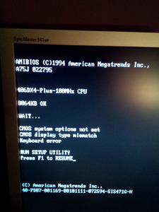
So your 486DX2-66&EW should be indicated as P24D, but the 80486DX2-S indication tells me this CPU is in WT mode! You should be able to confirm this with a CPU Identification tool like my CHKCPU.

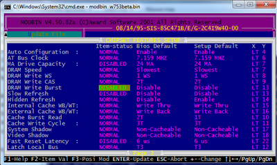
Note that this BIOS shows the “Internal Cache WB/WT:” option in the BIOS Setup only for the P24T and for Cyrix CPUs.
For the P24D (486DX2WB), iDX4WB, and Am486DX2WB/DX4WB, this 08/14/95 BIOS can detect if these CPUs are in WB mode and programs the chipset registers accordingly. It then hides the “Internal Cache WB/WT:” option, because user interaction for this automatic function is not required.

So, you only have to find the correct jumpers for L1 WB mode and the BIOS takes care of the rest. 😉

Jan

CPU Identification utility
The Unofficial K6-2+ / K6-III+ page

Reply 27 of 30, by Vasco

User metadata
Rank Newbie
Rank
Newbie

Hi Jan,

thanks for your feedback.

The JC4 jumper configurations had lots of similarities with the DACK0/1* hardware traps (disregarding actual hi/lo polarity), therefore I thought that'd be enough - apparently it's not.

After comparing jumper settings for "SX vs SX-SL", "DX vs DX-SL" and "SX vs DX" between MS-4138 (SiS47x) and MS-4144 (SiS49x) and also to P24T and/or DX4WB on the MS-4144 (which is mentioned there) - which have different jumper blocks but apparently following the same patterns for "SX vs DX" and "non-SL/Green vs SL/Green" etc. - I came to the conclusion, that one of the previously undocumented jumpers for the MS-4138 is simply missing being set.

Then again after trying some random combinations out at the JC1 and JC2 jumper blocks, setting JC1 (at the VLB slots) jumper J1-14 (the rightmost one) suddenly made the BIOS report a "P24D-S". \:D/
The L1 WB is enabled and the CPU correctly reports itself with CPUID 0x470 (=WB) instead of 0x463 (=WT), though the chipset's "L1 write burst" bit is still unset.
The BIOS entry regarding "Internal Cache WT/WB" is still inaccessible though, as you wrote.

The jumper JC4 which mentions "P24D/P24T" setting printed on the PCB when left open doesn't make a difference to the "SX/DX/SL/P24C" setting of 1-2 (the rightmost pins).

Cheers,
Vasco

Reality continues to ruin my life.

Reply 28 of 30, by Chkcpu

User metadata
Rank Member
Rank
Member

Hi Vasco,

Okay, you found the L1 cache WB jumper! 😀
Now that you have the CPU in L1 WB mode, a successful boot from a floppy is a great test to check if the other jumpers for the chipset’s HITM#, INV, and CACHE# lines are correctly set as well.

About the still disabled “L1 write burst” (SiS471 chipset Register 50h bit 1), this is controlled by the “DRAM Write Burst” option in the Award’s BIOS Chipset Features Setup menu.
However, when I look in the W753BETA BIOS with Modbin, I see that the Item-status of this option is DISABLED, so it is always hidden.

DRAM Write Burst.png
Filename
DRAM Write Burst.png
File size
55.84 KiB
Views
650 views
File license
Fair use/fair dealing exception

If you want it visible, set the Item-status to NORMAL, hit the Enter key to update this Menu page and save the changes when exiting Modbin. And of course, burn the changed BIN in an EPROM. 😉

Cheers, Jan

CPU Identification utility
The Unofficial K6-2+ / K6-III+ page

Reply 29 of 30, by Vasco

User metadata
Rank Newbie
Rank
Newbie

I tried to flip that bit manually via ctchips, but - depending on set jumpers on JC1, JC2 and JC4 - the box either (reproducably) freezes, reboots or continues to work normally.

The freeze and reboot behavior is highly jumper-config dependent (you'll change some and behavior goes from freeze to reboot and vice versa, as is the continuation (with ctchips reporting bit = 1).

Though I don't experience any differences.
Tried to reduce cache write states from 2->3 (single) / 1->2 (burst) - both are combined in a cfg bit - and the Speedsys write speed decreases as expected.

Strangely even with "L1 Write Burst" disabled, Speedsys shows a constant write speed of ~60MB/s - which matches the L1 read speed. L2 read speed is around 45MB/s (WT) and DRAM around 30MB/s (60ns FPM).
I have no idea why the L1/L2 caches don't have any effect on write speed, no matter WT or WB for L1 or L2 configured.

Maybe I should give modbin and my EPROMmer a try - maybe there's more to enable that feature besides flipping a bit.

Kind regards,
Vasco

Reality continues to ruin my life.

Reply 30 of 30, by Spitz

User metadata
Rank Member
Rank
Member
Vasco wrote on 2021-12-21, 21:56:
I tried to flip that bit manually via ctchips, but - depending on set jumpers on JC1, JC2 and JC4 - the box either (reproducabl […]
Show full quote

I tried to flip that bit manually via ctchips, but - depending on set jumpers on JC1, JC2 and JC4 - the box either (reproducably) freezes, reboots or continues to work normally.

The freeze and reboot behavior is highly jumper-config dependent (you'll change some and behavior goes from freeze to reboot and vice versa, as is the continuation (with ctchips reporting bit = 1).

Though I don't experience any differences.
Tried to reduce cache write states from 2->3 (single) / 1->2 (burst) - both are combined in a cfg bit - and the Speedsys write speed decreases as expected.

Strangely even with "L1 Write Burst" disabled, Speedsys shows a constant write speed of ~60MB/s - which matches the L1 read speed. L2 read speed is around 45MB/s (WT) and DRAM around 30MB/s (60ns FPM).
I have no idea why the L1/L2 caches don't have any effect on write speed, no matter WT or WB for L1 or L2 configured.

Maybe I should give modbin and my EPROMmer a try - maybe there's more to enable that feature besides flipping a bit.

Kind regards,
Vasco

Let me check my setup - I'll let You know about results.

Well... I miss 80/90s ... End of story