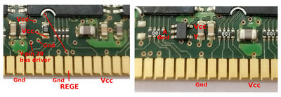
[edit: probably useful to note up here that I eventually figured out that all I'm doing is using the REGE pin 147 for its intend […]
Show full quote
[edit: probably useful to note up here that I eventually figured out that all I'm doing is using the REGE pin 147 for its intended purpose, to disable the register function, but keep the signals buffered]
(Short version: I accidentally got some registered RAM and converted it to unregistered)
I've just registered as I thought this might be of interest, and in case anyone has any suggestions about testing whether ECC is functioning on an Abit KA7 motherboard. Apologies if I break any etiquette.
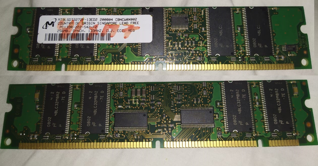
PC133r.jpg
Just been spending some time getting an Abit KA7 working again and was having trouble with the RAM. As part of an overly long story (including discovering that all the 3.3V on this board is regulated locally from PSU 12V, it doesn't use the PSU3.3V at all) I thought I'd try some ECC RAM (although I've since seen that the KX133 may not actually have implemented ECC correction anyway).
Problem was that I wasn't careful enough, and ended up getting some Micron PC133r probably from a Compaq server. And the KA7 doesn't support registered RAM (I think the extra clock tick delay mean data reads and writes don't line up). Having a quick look around it seemed that converting from registered to unregistered was a non-starter, so I'd have to look for some unregistered ECC ram.
That wasn't very common though, unlike all the ex-server stuff. So I had a closer look at the register chips on the sticks I had. In particular the 74ALVCF162835. Looked up a datasheet for it and in the second paragraph saw the following sentence:
"The device operates in Transparent Mode when LE is held HIGH."
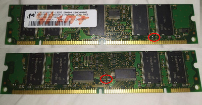
PC133r_Register.jpg
Well that sounded interesting. If the problem with using registered RAM was the delay caused by the register, then a non-clocked mode might help. I assumed (wrongly) that they'd have just tied the pin (28) low on each of the 3 registers, so I'd have to lift each pin and tie it high. Turns out all the pins were connected together, and I eventually found they were all connected to a pin on a small 5 pin device. That turned out to be a single bit inverter, the input of which was pulled high via a 10k resistor. Which means the output would be low, and the registers in clocked mode. But why go to that trouble? Turns out the input was also connected to pin 1467 on the DIMM, which I think is supposed to be NC. So it looks as though Micron wanted the motherboard to be able to switch the RAM between registered or unregistered. Which sounded hopeful.
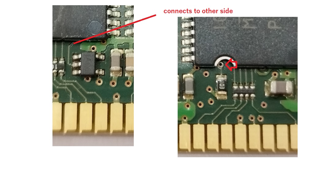
Just above the inverter were a couple of pads for an 0805 sized (I think) component and it turns out they go between the input and output of the inverter. So if I removed the inverter and shorted across the pads, then LE would be connected to pin 1467 (which should be NC) and a weak pull up to 3.3V. So I went ahead and did that.
PC133r_LE_Control.jpg
I guessed that I'd need to edit the SPD data stored on the DIMM, otherwise the motherboard would see that it said it was registered and not try to use the RAM. But I thought I'd just quickly try it first. And it booted. I assume BIOS writers do as little as possible to make things work, and checking to see whether or not you might be able to use the RAM, when you can just try it, is an extra step not needed.
So I now have buffered but unregistered ECC RAM. Of the 4 sticks I got, the 3 128MB ones all work at PC133/CL2 (tested one at a time, haven't tried installing all at the same time yet), but the 512MB one fails memtest86+ when run at PC133/CL3. It is stable at PC100/CL2 though.
Just tried installing edac_util in linux, but that just says "no memory controller data found". So probably no go with testing the ECC bit, unless anyone has any suggestions? I'll go with the '24 hours of memtest' instead.
So, for some registered RAM and some motherboards, converting from registered to unregistered just means removing one component and adding a short.