What a weird setup. I guess they wanted to save some pins on the main chip, since this is one-chip solution. But now the chipset has to scan all the DRQ lines in sequence.
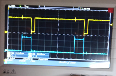
Oh well. Let's dig deeper into this. See if /E input of the '151 (pin 7) is connected to chipset or tied to GND permanently. Just so we know, it is working because SB test went fine. Then test inputs S0,S1,S2 (pins 11,10,9), you should see them toggling. All the time actually to properly scan all inputs, unless this chipset is "smart" and only scans the enabled DMA channels. But even in that case the S1 line should be toggling during floppy R/W attempts. Actually the combination should be LHL but you said low DRQ lines are connected to pins 12-15, which map to inputs 4 to 7. So possibly the S2 is permanently high and only S0 and S1 toggle? Again, weird setup. So the input for DRQ2 would be S0:L, S1:H, S2:H - you could maybe try a second scope channel to see if that is indeed what's on S0 and S2 when S1 goes high. In general S1 should toggle properly if DMA0 is working but better be sure.
Now, assuming S-inputs do toggle, then check if pins 5/6 (same output but negated on 6 and I'm not sure which one is connected to chipset, probably 6) toggle. Typically with no DMA activity the Z output should stay at the same level (Z=H, /Z=L because DRQ lines are all H) but then it should start toggling L during floppy access. It's not impossible that somehow only the DRQ2 input on this '151 chip is faulty (killed by ESD for example) and doesn't go through, but other DMA channels work. In fact if you don't see the Z output change you can retry this test with SoundBlaster again but monitor for it's DMA to see how this should be working.
Frankly if other DMA channels work (especially if you tested 0, 1 and 3), the '151 is driven properly, and passes correct signal to the output, and that line goes to chipset as it should. So the way I see it the only faults possible are:
- the '151 is partially damaged and only DRQ2 line is busted
- the chipset is "smart" and is not even scanning DMA channel 2 beause it's not enabled (but why would it not be for floppy transfer? wrong BIOS?)
Perhaps the DRQ2 connection to the '151 chip is so marginal it doesn't work properly (mobo damage somewhere) but then again I would exepct the signal to get trough eventually if you can trace the connection, and because this is request-acknowledge type of protocol it would make is slower in random ways, not stop it completly.

 "It's science. I ain't gotta explain sh*t"