VOGONS


First post, by jakethompson1

User metadata
Rank Oldbie
Rank
Oldbie

I saw the AMIBCP search thread was active again. In talking with some of the members about the PS/2 mouse hardware modifications on their boards, there are at least a few modifications you can do with these BIOSes even without having AMIBCP, found by digging around in the hex dump, DOS DEBUG, and in IDA Free edition.

These BIOSes are exactly 64K and are not compressed. You know you have a compressed BIOS if it will not allow you to disable BIOS Shadowing. WinBIOSes, unfortunately, are compressed so this works only on older ones. For this example I am using one of the 08/08/93 BIOSes and I'm running it inside PCem "ami486" machine for testing. You could also do this on real hardware but you will have to keep flashing the BIOS chip to make any changes.

Patching out checksum verification code
The first hurdle is that any modifications to the BIOS will invalidate its checksum. These BIOSes validate their checksum by adding up the BIOS contents, 16 bits at a time discarding overflow, and checking that the result sums to zero. By using the Search command in DOS debug we can find this code and use the Unassemble command to verify it's right:

A:\>debug
-S F000:0 L FFFF 2E AD 03 D8 E2 FA
F000:DC9A
-U F000:DC9A
F000:DC9A 2E CS:
F000:DC9B AD LODSW
F000:DC9C 03D8 ADD BX,AX
F000:DC9E E2FA LOOP DC9A
F000:DCA0 7406 JZ DCA8

The JZ instruction jumps to DCA8 if the checksum passes. If the checksum fails, the BIOS continues straight ahead with code I haven't shown, presumably code to beep the PC speaker and loop.

By changing the byte at location DCA0 from 74 to EB, we change JZ to JMP. This makes it so that the BIOS no longer cares whether the checksum is right. Note that we don't actually know where the checksum is. Because it is only verifying that the BIOS contents add up to zero, it could be anywhere.

You must do this before you can make any other modifications.

Enabling PS/2 mouse support
By default PCem will not let you attach a PS/2 mouse to the ami486 machine. By editing src/model.c, going to "[486] AMI 486 clone" line, and adding |MODEL_PS2 after ...MODEL_HAS_IDE and recompiling, it will let you.

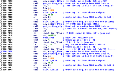
After doing that, and attaching a PS/2 mouse in the settings, you may find that mouse drivers report no PS/2. You can try AMISETUP but it won't help. This is because there seems to be a byte in the AMIBIOS that controls various things like whether there is a PS/2 mouse port on the board. We can find it using debug.

INT 15 with AX=C204h asks the BIOS what type of mouse is connected. Start debug, Assemble, and enter the instructions to trigger this interrupt.

A:\>debug
-A
1C27:0100 MOV AX,C204
1C27:0103 INT 15
1C27:0105
-

Now, we want to trigger this interrupt and keep Tracing through the BIOS code until we see a TEST BYTE PTR [....],10 instruction. It may take 10-20 instructions so be patient. This byte seems to be ORed with 0x10 if a PS/2 mouse port is present, and because it is in ROM and not in CMOS, no amount of tweaking in CMOS Setup can change it.

...
AX=C242 BX=0000 CX=0000 DX=0000 SP=FFE6 BP=0000 SI=0000 DI=0000
DS=1C27 ES=1C27 SS=1C27 CS=F000 IP=9741 NU UP EI PL NZ NA PE NC
F000:9741 3C12 CMP AL,12
-T

AX=C242 BX=0000 CX=0000 DX=0000 SP=FFE6 BP=0000 SI=0000 DI=0000
DS=1C27 ES=1C27 SS=1C27 CS=F000 IP=9743 NU UP EI PL NZ NA PE NC
F000:9743 735C JNB 97A1
-T

AX=C242 BX=0000 CX=0000 DX=0000 SP=FFE6 BP=0000 SI=0000 DI=0000
DS=1C27 ES=1C27 SS=1C27 CS=F000 IP=97A1 NU UP EI PL NZ NA PE NC
F000:97A1 3C40 CMP AL,40
-T

AX=C242 BX=0000 CX=0000 DX=0000 SP=FFE6 BP=0000 SI=0000 DI=0000
DS=1C27 ES=1C27 SS=1C27 CS=F000 IP=97A3 NU UP EI PL NZ NA PO NC
F000:97A3 75B1 JNZ 9756
-T

AX=C242 BX=0000 CX=0000 DX=0000 SP=FFE6 BP=0000 SI=0000 DI=0000
DS=1C27 ES=1C27 SS=1C27 CS=F000 IP=9756 NU UP EI PL NZ NA PO NC
F000:9756 2E CS:
F000:9757 F606808210 TEST BYTE PTR [8280],10 CS:8280=2F

Notice that [8280] holds the value 2F, which when ANDed with 10, will produce zero. This means that the byte in the BIOS at offset 8280 needs to be changed from 0x2F to 0x3F (i.e. OR it with 0x10). The PS/2 mouse port will then be enabled.

After making those two modifications on this particular BIOS, and the hack to PCem, I can use a PS/2 mouse even though the board this BIOS belongs to did not have one. Of course, to do this on real hardware, you would have to do the keyboard controller hack described by feipoa, maxtherabbit et al.

Un-hiding options in SETUP
If you scroll through the BIOS using your hex editor, you will eventually come across a region of bytes with hex values 00, 01, 02, 03, 04, ...

Immediately after that is a table of choice strings. This lets BIOS SETUP map numeric choices (0, 1, 2, ...) to the strings that show in SETUP such as Reserved, Disabled, Enabled, Absent, ...

Immediately after that are the actual settings: Typematic Rate Programming, Typematic Rate Delay, etc.

The format of each setting is:
a string describing the setting followed by a 00 byte.
a byte identifying which CMOS register is controlled by the setting. Because registers go only from 0x00 to 0x7f, bit 7 is used to control whether the setting is shown or not.
other bytes not relevant here.

In this particular BIOS, the AUTO Config Function, Cache Read Option, Cache Write Option, DRAM Type, and DRAM Wait State(s) options are all hidden. To show them, I will have to change the byte at 0xc55b from 0x54 to 0xd4, the byte at 0xc57b from 0x41 to 0xc1, the byte at 0xc59b from 0x41 to 0xc1, the byte at 0xc5bb from 0x41 to 0xc1, and the byte at 0xc5db from 0x41 to 0xc1 (i.e. OR them with 0x80).

0000c530: 61 74 65 20 20 20 00 b5 60 00 04 2d 2c 2b 2a 41 ate ..`..-,+*A
0000c540: 55 54 4f 20 43 6f 6e 66 69 67 20 46 75 6e 63 74 UTO Config Funct
0000c550: 69 6f 6e 20 20 20 20 20 20 20 00 54 40 0f 00 20 ion .T@..
0000c560: 20 20 20 20 20 43 61 63 68 65 20 52 65 61 64 20 Cache Read
0000c570: 4f 70 74 69 6f 6e 20 20 20 20 00 41 c0 10 00 20 Option .A...
0000c580: 20 20 20 20 20 43 61 63 68 65 20 57 72 69 74 65 Cache Write
0000c590: 20 4f 70 74 69 6f 6e 20 20 20 00 41 30 11 00 20 Option .A0..
0000c5a0: 20 20 20 20 20 44 52 41 4d 20 54 79 70 65 20 20 DRAM Type
0000c5b0: 20 20 20 20 20 20 20 20 20 20 00 41 04 13 00 20 .A...
0000c5c0: 20 20 20 20 20 44 52 41 4d 20 57 61 69 74 20 53 DRAM Wait S
0000c5d0: 74 61 74 65 28 73 29 20 20 20 00 41 03 12 00 20 tate(s) .A...

After changing those, the settings are unhidden in the Advanced Chipset Setup.

To do
I believe the Power on Default and CMOS Setup default values are stored nearby.
Has anyone run into entire menus (eg Advanced Chipset Setup) being disabled-I believe I did on someone's BIOS and was able to unhide it.
Figure out WinBIOS-it may be a big undertaking.
Based on this experience, the AMISETUP author either had documentation about these BIOSes, or did the same steps described here (including on later BIOSes like WinBIOS). It might be possible to contact the AMISETUP author if he would be willing to provide any more info.

Reply 2 of 26, by Tiido

User metadata
Rank l33t
Rank
l33t

This is great ~

T-04YBSC, a new YMF71x based sound card & Official VOGONS thread about it
Newly made 4MB 60ns 30pin SIMMs ~
mida sa loed ? nagunii aru ei saa 😜

Reply 3 of 26, by Eep386

User metadata
Rank Member
Rank
Member

Thank you very much for posting this!

Life isn't long enough to re-enable every hidden option in every BIOS on every board... 🙁

Reply 4 of 26, by feipoa

User metadata
Rank l33t++
Rank
l33t++

Nice to see this information retained online now. It is probably too involved for most users of the forum, but that could change in time.

Plan your life wisely, you'll be dead before you know it.

Reply 5 of 26, by hyoenmadan

User metadata
Rank Member
Rank
Member

Just for the record... Combining this technique with MyBCP from Herbert Oppmann (which can uncompress even MAIN module) would make it work for compressed AMIBIOS6 cores, which don't work or get corrupted by AMI BCP7 tools (BCP, MM and OLG logo encoding tools), as long the changes don't mess with the module relocation table contained in MAIN.

Reply 6 of 26, by SSTV2

User metadata
Rank Oldbie
Rank
Oldbie

*** A small off-topic ***

Interesting, I've never had a need to modify an AMI BIOS before, thus most of what was mentioned here was new to me, especially the checksum calculation. I've read on Vogons before, that the AMI BIOS checksum patching is somewhat difficult or unusual and now I see why is that. The whole process doesn't follow a standard checksum calculation method, where every byte is added sequentially and the end result is compared with a specific checksum byte value, instead it adds all 16 bit words sequentially. You might think at first that it's just a simple 16 bit checksum calculation that many HEX editors can easily perform, but that would be a false assumption, because a 16 bit checksum operation also follows a standard checksum calculation method, except you get an additional high byte on top of an 8 bit checksum value.

I'll give an example, lets say we have these values:

ASCII: 0 1 2 3 4 5 7 6 8 9 A B C D E F
HEX: 30 31 32 33 34 35 36 37 38 39 41 42 43 44 45 46 (LOW, HIGH, LOW, HIGH... bytes)

These would be the checksums of:

8bit operation  - 30+31+...+46      =   A2 H
16bit operation - 30+31+...+46 = 03A2 H
What AMI used - 3130+3332+...4645 = D6CD H

Now knowing how the checksum calculation is actually performed for the AMI BIOS, it doesn't look too difficult to properly patch it, except for one small detail, which was already mentioned by jakethompson1, it's not clear where the actual checksum correction word is.

*** on-topic ***

I know that C2h function of INT15h is essential for the BIOS's PS/2 mouse support, do you know how to check whether that function is present in the AMI BIOS image using a hex editor/debug? I had one case where an AWARD BIOS lacked that function completely, thus PS/2 mouse didn't work even after enabling PS/2 mouse in the BIOS configuration byte (after driver load a cursor would show up in DOS programs, but it wouldn't react to mouse movements). Motherboard was fully PS/2 capable.

Reply 7 of 26, by jakethompson1

User metadata
Rank Oldbie
Rank
Oldbie
feipoa wrote on 2021-07-11, 05:34:

Nice to see this information retained online now. It is probably too involved for most users of the forum, but that could change in time.

Now you know what it's like for us reading your directions on upgrading the 8433UUD to 1024k cache, modifying the keyboard controller to add a mouse port, etc. "Just add an X ohm resistor here, a capacitor here, run a wire from pin X to Y, etc."..... huh? 😁

This process could be automated. One reason I hesitate to is there are too many heuristics now e.g. "there's a table of option names followed by X" which may not always be true across all versions.

Reply 8 of 26, by feipoa

User metadata
Rank l33t++
Rank
l33t++

I do plan on updating those directions, but I'm not sure when. I've since made it possible via jumpers to switch between 256K, 512K, and 1024K, all double-banked. I've been running the newly mod board without any issues for some time now, currently with 512K double-banked at 66 MHz. The existing Biostar manual v2 should have sufficient photographs and written detail for the 1024K mod, but perhaps nobody else has done the mod yet because everyone wants a video these days.

Plan your life wisely, you'll be dead before you know it.

Reply 9 of 26, by bakemono

User metadata
Rank Oldbie
Rank
Oldbie
SSTV2 wrote on 2021-07-12, 00:53:

Now knowing how the checksum calculation is actually performed for the AMI BIOS, it doesn't look too difficult to properly patch it, except for one small detail, which was already mentioned by jakethompson1, it's not clear where the actual checksum correction word is.

A sum of 16-bit words is not all that unusual, I know I've seen it before (eg. Sega games). Save files for PC games often use a sum of 32-bit words.

Not knowing where the BIOS originally had it checksum fixed doesn't stop us from fixing it again though. Just choose a location that doesn't appear to be used for anything else, such as inside a big block of zeros or an ASCII string that nobody cares about.

again another retro game on itch: https://90soft90.itch.io/shmup-salad

Reply 10 of 26, by jakethompson1

User metadata
Rank Oldbie
Rank
Oldbie

So on archive.org there are some archived manuals from ftp.megatrends.com. There are many references to AMIBCP, and even some screenshots, but no AMIBCP itself. Still, it was helpful to better understand some of these old BIOSes.

Other sources, including UMB_DRVR, suggest that 0000h-7fffh in these BIOSes is used for the BIOS setup program and POST, while 8000h-ffffh is used at runtime. That seems consistent with what I see.

In particular, the BIOS starting at 8000h, for the 08/08/93 BIOS, seems to have a quite structured layout. The other dates are likely similar. Note that this was a BIOS without support for an onboard I/O controller and extra setup menu screen to configure it. Some of the gaps in the memory layout are likely filled in with such settings for a BIOS with onboard I/O settings.

8000h - ROM copyright string
8050h - secondary ROM copyright string
8078h - BIOS string 1
80a0h - BIOS string 2 (shows up with Ins key)
80c8h - BIOS string 3 (shows up with Ins key)
80f0h - Power-on copyright banner
8200h - Standard CMOS defaults as a binary image ready to be copied into registers. Partly redundant with default tables later on.
8240h - I/O addresses to probe for serial ports
8248h - I/O addresses to probe for parallel ports
8250h - unknown POST-related flags
825eh - scan code for Ctrl-Alt-____ turbo-on hot key
826eh - scan code for Ctrl-Alt-____ turbo-off hot key
8280h - BIOS options flags (editable using AMIBCP)
80h - halt on error during POST
40h - initialize CMOS on every boot
20h - KBC output pin 23,24 blocked
10h - Mouse support in BIOS/KBC
08h - Wait for <F1> on POST error
04h - Display floppy error during POST
02h - DIsplay video error during POST
01h - Display keyboard error during POST
8281h - BIOS flags (not editable using AMIBCP)
02h - power management supported?
40h - 80286 CPU?
80h - evaluation copy
8282h - Shown/hidden settings for entire submenus of CMOS Setup program
8284h - Power on delay
8285h - Software i/o delay?
8286h - Refresh value?
8290h - Pointer to setup program settings indexes table
8292h - Pointer to choice, choice callback, setup program settings table
8294h - Pointer to CMOS Defaults table
8296h - Pointer to Chipset Defaults table
8298h - Pointers to unknown defaults table (possibly power management related)
829ch - Pointers to table of lengths of other tables
82a0h - Pointers to floppy controller configuration tables for 360k-1.44M floppy disk sizes
82aah - Pointer to unknown function
82ach - Pointer to floppy controller configuration table for 2.88M floppy disk size
82b1h - Pointer to maximum register stored in default tables
82b3h - Maximum CMOS register number to include in checksum computation
82b6h - Pointers to unknown functions
82f0h - begin AMI Green PC power management related settings

Finally it also appears that the two-byte checksum is most likely stored at ff50h.

Reply 11 of 26, by AlexZ

User metadata
Rank Member
Rank
Member

Emulators are great for debugging and patching BIOSes. No harm done if something breaks. If your board has chipset supported in emulator, you should be able to copy your BIOS in there and it should work.

Pentium III 900E, ECS P6BXT-A+, 384MB RAM, NVIDIA GeForce FX 5600 128MB, Voodoo 2 12MB, 80GB HDD, Yamaha SM718 ISA, 19" AOC 9GlrA
Athlon 64 3400+, MSI K8T Neo V, 1GB RAM, NVIDIA GeForce 7600GT 512MB, 250GB HDD, Sound Blaster Audigy 2 ZS

Reply 12 of 26, by jakethompson1

User metadata
Rank Oldbie
Rank
Oldbie
AlexZ wrote on 2021-08-28, 04:29:

Emulators are great for debugging and patching BIOSes. No harm done if something breaks. If your board has chipset supported in emulator, you should be able to copy your BIOS in there and it should work.

Yes, agreed. The old AMIBIOSes that are 64K and that do not have to decompress themselves into RAM often work even with the "wrong" chipset in PCem. Once you get into the ones that are compressed, which tends to show up around the same time as WinBIOS, PCI, and ISA Plug n Play support, the chipset has to match because they have to set up shadow RAM in order to do the decompression.

Reply 13 of 26, by GigAHerZ

User metadata
Rank Oldbie
Rank
Oldbie

Have you compared the list of options you've found with the list of options you could enable through AMISETUP?
Any additional features that could be enabled, that AMISETUP can not do?

"640K ought to be enough for anybody." - And i intend to get every last bit out of it even after loading every damn driver!

Reply 14 of 26, by jakethompson1

User metadata
Rank Oldbie
Rank
Oldbie
GigAHerZ wrote on 2021-08-28, 08:59:

Have you compared the list of options you've found with the list of options you could enable through AMISETUP?
Any additional features that could be enabled, that AMISETUP can not do?

The biggest one so far is that a handful of posters have done a hardware modification to keyboard controllers that are already capable of driving a PS/2 mouse, to add a PS/2 mouse port to boards that don't come with one. The hidden Mouse Support Option setting, that you can change using AMISETUP, is not enough on its own. The mouse support is blocked from taking effect unless the appropriate bit at 8280h is set.

Reply 15 of 26, by GigAHerZ

User metadata
Rank Oldbie
Rank
Oldbie
jakethompson1 wrote on 2021-08-28, 20:08:
GigAHerZ wrote on 2021-08-28, 08:59:

Have you compared the list of options you've found with the list of options you could enable through AMISETUP?
Any additional features that could be enabled, that AMISETUP can not do?

The biggest one so far is that a handful of posters have done a hardware modification to keyboard controllers that are already capable of driving a PS/2 mouse, to add a PS/2 mouse port to boards that don't come with one. The hidden Mouse Support Option setting, that you can change using AMISETUP, is not enough on its own. The mouse support is blocked from taking effect unless the appropriate bit at 8280h is set.

Beautiful find! Thanks!

"640K ought to be enough for anybody." - And i intend to get every last bit out of it even after loading every damn driver!

Reply 16 of 26, by TheMobRules

User metadata
Rank Oldbie
Rank
Oldbie

First of all, I'm sorry about resurrecting this thread, but I wanted to thank @jakethompson1, as this has been extremely useful for some BIOS tinkering I've been doing.

Also, I wanted to discuss certain details about what is mentioned in the section "Un-hiding options in SETUP":

jakethompson1 wrote on 2021-07-08, 01:40:

a byte identifying which CMOS register is controlled by the setting

So, currently I'm troubleshooting a 486 BIOS (08/08/1993 core) and I've noticed that it completely ignores a couple of settings related to timings: Cache Burst Read Cycle, which always is set to 2T despite setting 1T in the CMOS setup, and Bus Clock Frequency Select, which also ignores the user setting and is fixed at 7.159... MHz instead of using the Bus clock frequency dividers. I'm using CTCHIP34 to verify that these chipset register values remain unchanged at all times no matter if I change them in the CMOS setup. Other registers for timings and options are set correctly according to the option chosen in setup.

Now, since it's a VLB motherboard having a slightly slower ISA bus speed is not of great concern, but the inability to set 1T on the Cache Burst Read Cycle has an effect so notorious that L2 cache is not detected when setting main memory to the tightest timings, due to the small differences between those speeds.

Returning to the BIOS modding, I've noticed that the CMOS register number where these options are set is not the same as the chipset register number that is affected (for instance, in the BIOS setup the CMOS register for the cache timings is 36h, but the chipset register that handles this in the SiS471 chipset is 51h). So, I assume there has to be a mapping between the CMOS register values that are set on the SETUP utility and the chipset register so the chipset is configured at boot time right? I assume this is where the BIOS issue would be, but I'm not so sure where I could start looking for this. Any help or suggestions are welcome!

By the way, I've noticed that in addition to the first byte being the CMOS register that is controlled by the option (including whether it's hidden or not), the following byte indicates which bits of the register are affected by the setting. Not sure about the 3rd byte, but the 4th indicates the number of options for that setting and after that there is one byte per each option that points to entries in the table mentioned by jakethompson1 that maps all the different options with their labels.

Reply 17 of 26, by jakethompson1

User metadata
Rank Oldbie
Rank
Oldbie
TheMobRules wrote on 2023-02-06, 19:23:
First of all, I'm sorry about resurrecting this thread, but I wanted to thank @jakethompson1, as this has been extremely useful […]
Show full quote

First of all, I'm sorry about resurrecting this thread, but I wanted to thank @jakethompson1, as this has been extremely useful for some BIOS tinkering I've been doing.

Also, I wanted to discuss certain details about what is mentioned in the section "Un-hiding options in SETUP":

jakethompson1 wrote on 2021-07-08, 01:40:

a byte identifying which CMOS register is controlled by the setting

So, currently I'm troubleshooting a 486 BIOS (08/08/1993 core) and I've noticed that it completely ignores a couple of settings related to timings: Cache Burst Read Cycle, which always is set to 2T despite setting 1T in the CMOS setup, and Bus Clock Frequency Select, which also ignores the user setting and is fixed at 7.159... MHz instead of using the Bus clock frequency dividers. I'm using CTCHIP34 to verify that these chipset register values remain unchanged at all times no matter if I change them in the CMOS setup. Other registers for timings and options are set correctly according to the option chosen in setup.

Now, since it's a VLB motherboard having a slightly slower ISA bus speed is not of great concern, but the inability to set 1T on the Cache Burst Read Cycle has an effect so notorious that L2 cache is not detected when setting main memory to the tightest timings, due to the small differences between those speeds.

Returning to the BIOS modding, I've noticed that the CMOS register number where these options are set is not the same as the chipset register number that is affected (for instance, in the BIOS setup the CMOS register for the cache timings is 36h, but the chipset register that handles this in the SiS471 chipset is 51h). So, I assume there has to be a mapping between the CMOS register values that are set on the SETUP utility and the chipset register so the chipset is configured at boot time right? I assume this is where the BIOS issue would be, but I'm not so sure where I could start looking for this. Any help or suggestions are welcome!

By the way, I've noticed that in addition to the first byte being the CMOS register that is controlled by the option (including whether it's hidden or not), the following byte indicates which bits of the register are affected by the setting. Not sure about the 3rd byte, but the 4th indicates the number of options for that setting and after that there is one byte per each option that points to entries in the table mentioned by jakethompson1 that maps all the different options with their labels.

Silly question--there is sometimes an Auto Configuration option that could itself be hidden, that might account for what you're seeing. You might want to try AMISETUP before going straight to modding the BIOS.

You're right that often the chipset register and CMOS register numbers don't match, especially when multiple on/off settings are packed into the bits of a CMOS register value and have to be unpacked in order to program the chipset registers. I don't think there is an easy mapping that you could handle with a table; this was all handled in code on a per chipset basis. Now the question is whether AMI/Award did all the programming on their own or offered a "link kit" where chipset vendors could plug in the needed modules to program their chipsets. Once you go past ISA/VLB the BIOSes get even harder to understand.

Reply 18 of 26, by TheMobRules

User metadata
Rank Oldbie
Rank
Oldbie
jakethompson1 wrote on 2023-02-08, 23:03:

Silly question--there is sometimes an Auto Configuration option that could itself be hidden, that might account for what you're seeing. You might want to try AMISETUP before going straight to modding the BIOS.

You're right that often the chipset register and CMOS register numbers don't match, especially when multiple on/off settings are packed into the bits of a CMOS register value and have to be unpacked in order to program the chipset registers. I don't think there is an easy mapping that you could handle with a table; this was all handled in code on a per chipset basis. Now the question is whether AMI/Award did all the programming on their own or offered a "link kit" where chipset vendors could plug in the needed modules to program their chipsets. Once you go past ISA/VLB the BIOSes get even harder to understand.

It's been some time, but during the last few days I had the chance to work on this and wanted to give some closure to my previous post, I've learned a few things in the process that may be of help for fellow AMI BIOS modders (at least until a suitable version of AMIBCP for these old BIOSes is found).

First of all, some context: I have an MSI SiS471-based 486 VLB board, the MS-4132G ver. 1. The original AMI BIOS that came with this board (version A75A) had a few issues, some of which resulted in generally mediocre performance:

  • The Cache Burst Read Cycle option was stuck at 2T regardless if 1T was selected in the BIOS setup, making it impossible to set 2-1-2 timings and having to settle on 2-2-2
  • The Bus Clock Frequency Select was also fixed to 7.159MHz, selecting a divider like 1/4 BUSCLK had no effect at all
  • There was no option for using 1 bit of the tag SRAM for the dirty bit with L2 WB cache, resulting in abysmal memory performance due to the "always dirty" cache policy
  • The T2/T3 and SYNC/TRANSPARENT options were inverted, i.e. if you select T2 the BIOS actually sets T3 and vice-versa, same for SYNC/TRANSPARENT

The last one is purely cosmetic, but the others do affect system performance (the dirty bit problem is common on SiS471 boards, even on Award BIOS but those can be easily modded). Luckily I got a dump of a slightly newer BIOS (version A75B) from fellow vogoner @leonardo, where MSI seems to have fixed the dirty bit and the Bus Clock Frequency selection, but the other two problems remain. So, I decided to try and fix those.

The inverted options bug was a piece of cake with the tips provided by @jakethompson1, it was just a matter of finding the section with all the options and I just swapped the values.

The Cache Burst Read Cycle problem was not that simple. First, I confirmed with both CTCHIP34 and a small assembly program I wrote that the register bit for this option (reg. 51 bit 0) was being always set to 1 (2T). Then, with AMISETUP I found that when I select the "1T" option in the BIOS SETUP program the value written to the corresponding CMOS register (reg. 36h bit 5) is set to the correct value (0). So, this means that for some reason the BIOS is not setting this bit properly when configuring the chipset during the boot process.

With the free IDA disassembler and some patience I attempted to find the section in the code where the SiS471 is programmed with the settings from the CMOS. I quickly realized that following the entire boot process from the very start would take an eternity, so first I focused on trying to find writes to the I/O ports 22h and 23h, which are used to configure the SiS471 registers according to the datasheet. This yielded some promising results, but it was still difficult to see in what part of the boot process these writes were being executed. I had to find a better way, so I thought about POST codes (writes to I/O port 80h), and the "AMI Color" section of this page was extremely helpful:

AMI BIOS Post Codes

I figured it was better to focus on the last few codes when the BIOS is about to transfer control to the boot device, since I knew the L2 cache is enabled somewhat late in the process and this was probably where the timings are configured. I tried a few without success but this one did the trick:

A4 - Set memory wait states

A search for the following pair of instructions quickly led to results:

mov al, 0A4h
out 80h, al

Now, this post is getting too long and I'm a bit tired, so tomorrow I will post details on how the BIOS looks up the settings in the config table and retrieves the corresponding values from the CMOS to configure the chipset, and how I was able to identify the issue with the cache timing setting.

Reply 19 of 26, by TheMobRules

User metadata
Rank Oldbie
Rank
Oldbie

Continued from previous post.

Immediately after writing the "A4" POST code, the BIOS jumps to the following section where cache and DRAM memory timings are configured with the CMOS settings:

MS-4132G_CacheTimingsConfig.png
Filename
MS-4132G_CacheTimingsConfig.png
File size
102.13 KiB
Views
1200 views
File comment
Cache timings configuration code
File license
Public domain

Broadly speaking, each setting is configured in the chipset by following these steps:

  • First, the position of the setting in the BIOS table described by @jakethompson1 is written to AL
  • A routine I've called get_setting_cfg looks up the CMOS record for this setting and bits affected in the table and reads the actual value from the CMOS
  • When get_setting_cfg returns, it leaves the bits from the CMOS setting value in AL (shifted to the rightmost position)
  • The setting bits in AL are then shifted to the appropriate position as expected in the corresponding SiS471 register they will be written to
  • The current value of the appropriate SiS471 register is read (sis471_read, by first writing the register value to port 22h and then reading 23h)
  • The register value is updated with the configuration bits read from CMOS and written back to the chipset (sis471_write)

For example, in the code above the Cache Write Cycle Option is written by first loading AL with the setting position in the table (25h, Typematic Rate Programming would be 0, Typematic Rate Delay would be 1, etc.). Then, as described above the setting is retrieved from the CMOS and written to bit 1 of SiS471 register 51h.

However, the Cache Burst Read Option is not written immediately after this, instead 3 checks are performed (positions 2112 to 212C in the code). If any of these checks fail, the BIOS jumps to the next settings (DRAM speed and wait states, cache type and all that) without writing the Cache Burst Read Option. I figured this was the reason this setting was not being configured with the value specified in the BIOS SETUP, so let's take a look at what these 3 checks are:

  1. [2112-211C] DRAM speed must be 10 (Fast) or 11 (Fastest)
  2. [211E-2126] Bit 2 of CMOS register 33h must be 0
  3. [2128-212C] Result of reading port 22h bit 0 must be 1

Now, I'm not sure what the last two options mean, but in any case my assumption was that one of those checks was failing, so I wrote a small assembly program that tests those values and bingo! The last one, where port 22h is read and a value of 1 is expected in bit 0 did not pass.

Since the value read from 22h is immediately discarded and not used anywhere else, this check must not affect anything else in the code. So, the patch was easy: I just replaced the JZ instruction that jumps away with a couple of NOPs, since the 1T timing for Cache Burst Read should be easily achievable with 15ns:

MS-4132G_CacheTimingsPatch.png
Filename
MS-4132G_CacheTimingsPatch.png
File size
38.06 KiB
Views
1200 views
File comment
Cache timings patch
File license
Public domain

This did the trick! Now the board performs as expected and is on par with the fastest SiS471 boards out there! It may even work on other SiS471 boards if you're feeling adventurous.

Still, the question remains what is the purpose of reading port 22h? The SiS471 doc only makes reference to writing to 22h since it's the index used to specify which chipset register you want to access (by reading or writing to 23h afterwards). If anyone has any idea, I'd like to know.

Also, in the process I've learned a few more things, so if anyone is interested in specific aspects such as how the settings table is accessed let me know and I can go into more detail.

By the way, after patching the BIOS, instead of updating the code that calculates the checksum, I adjusted the word at FF50 (as suggested by @jakethompson1) so that the checksum is 0000, worked perfectly. An easy way to compute the checksum is with HxD, go to Analysis -> Checksums, in "Available algorithms" select "Custom checksum", then click on "Custom checksum" button and select: result bid width = 16, bit width = 16, Little Endian.

Attachments

  • Filename
    A75B.zip
    File size
    88.5 KiB
    Downloads
    30 downloads
    File comment
    MS-4132G A75B original & patched BIOS
    File license
    Fair use/fair dealing exception