First post, by stamasd
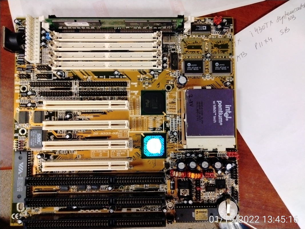
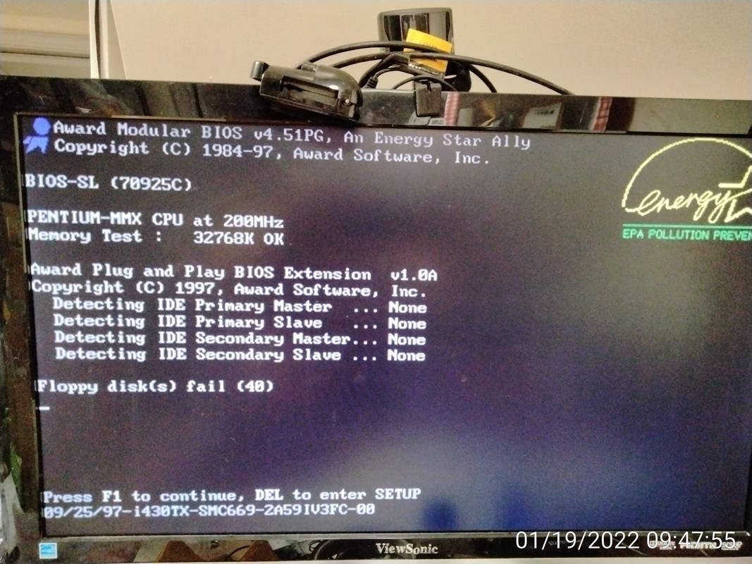
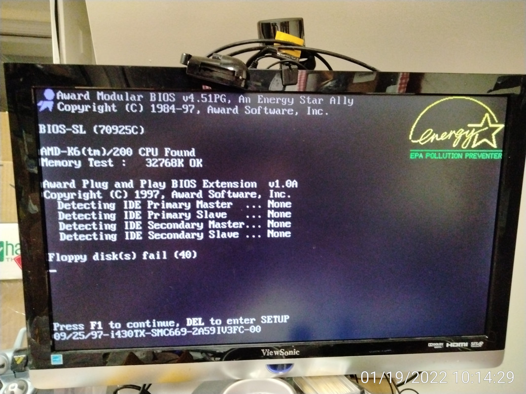
I just acquired (yet another) socket7 motherboard. This one caught my eye as it was listed on ebay under the wrong category (I was browsing vintage macintosh hardware) and fairly cheap. I did some investigating before buying, and it looked almost the same as the one posted here: https://www.ultimateretro.net/en/motherboards/5962 - even the same part number, but with an important difference: a wider variety of FSB choices. So I bought it, got it in the mail last night and started testing. The board appears to be in pristine condition, and I'd venture to say unused. I replaced the CMOS battery (CR2032, none of the barrel nonsense), added a P200MMX after setting the jumpers, and a 32MB stick of SDRAM, and it posted right away.
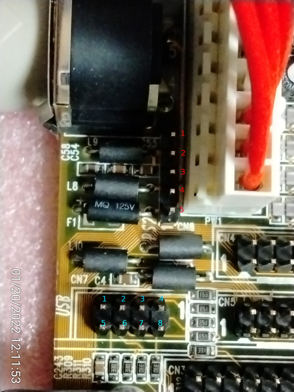
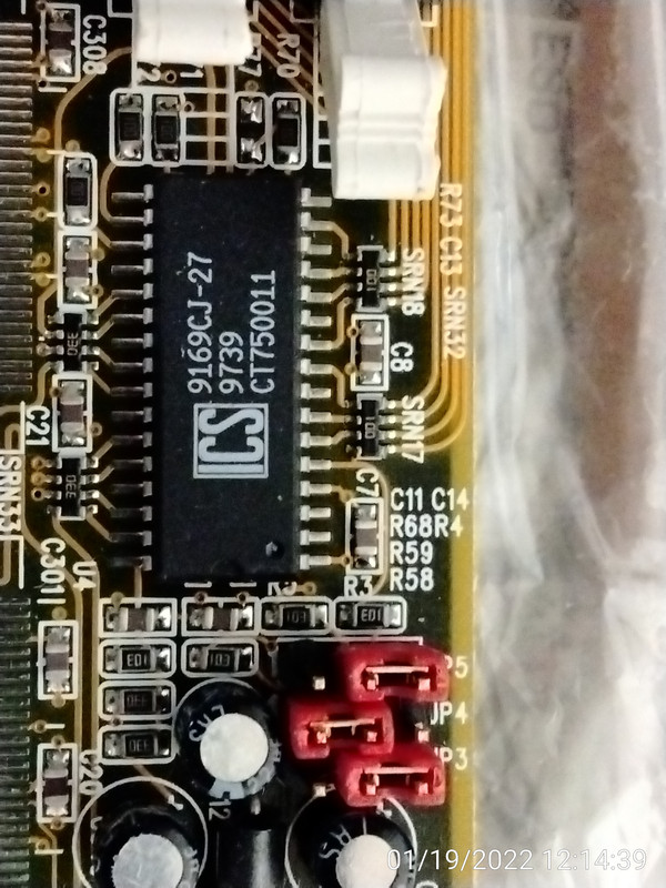
Now, the nice part is that it features a range of FSB choices from 50MHz to 83MHz because it has a different clock generator from the one posted on the ultimateretro website. Here is the datasheet of the chip https://pdf1.alldatasheet.com/datasheet-pdf/v … S9169CJ-27.html confirming that it can do (as silkscreened on the motherboard) 50/55/60/66/75/83MHz. It's also interesting that the chip can do async PCI clock of 32MHz independent of the FSB if configured correctly - and it looks like a 10kohm resistor is all that's needed to enable this if needed. I did test it up to 83FSB/41.5PCI which the Matrox G200 I was using had no trouble with - but other PCI cards may not fare that well.
I tested with a total of 3 CPUs which I had handy: a P200MMX, a K6-233 and a K6-166.
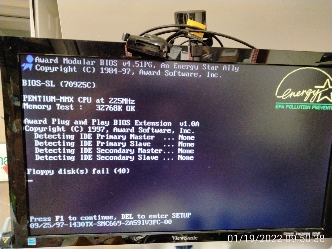
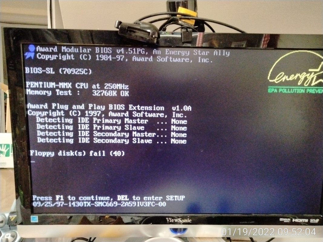
I tried the P200MMX at various FSBs, max I got was 250MHz (83x3) and min 150MHz (50x3) as the multiplier is locked. I did not need to change the default voltage of 2.8V for either.
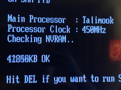
75MHz FSB
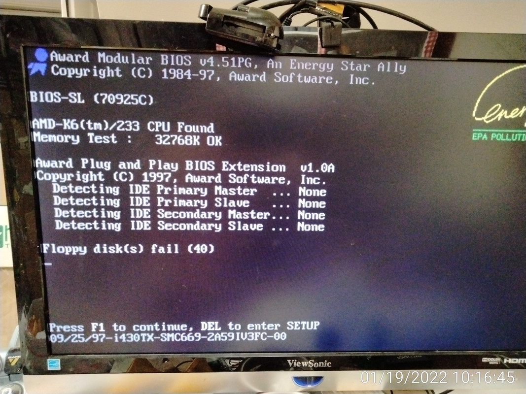
83MHz FSB
The K6-233 is not multiplier locked, and it interprets the 1.5x multiplier as 3.5, so I couldn't get the speed down too low unfortunately. Min speed I got was 100MHz (50x2), max was 266MHz (75x3.5). The K6-233 did NOT post at all with 83MHz bus, regardless of voltage. The only exception was 83x2 when it posted as a K6-166 at its default voltage (3.2V). It did not post at 83x2.5 or above even at 3.5V. I was hoping to get to 83x3.5=290MHz, but this CPU didn't live up to my dream. 😀
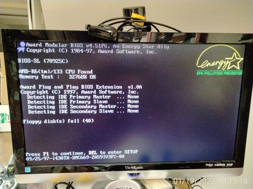
The only reason I tried a K6-166 was because I didn't remember if it also interpreted the 1.5x multiplier as 3.5x or not. Was hoping to go down as low as 50X1.5=75MHz, but it didn't happen. On the K6-166, the 1.5 is still read as 3.5.
And here's what the PCI/AGP snooper says about the board:
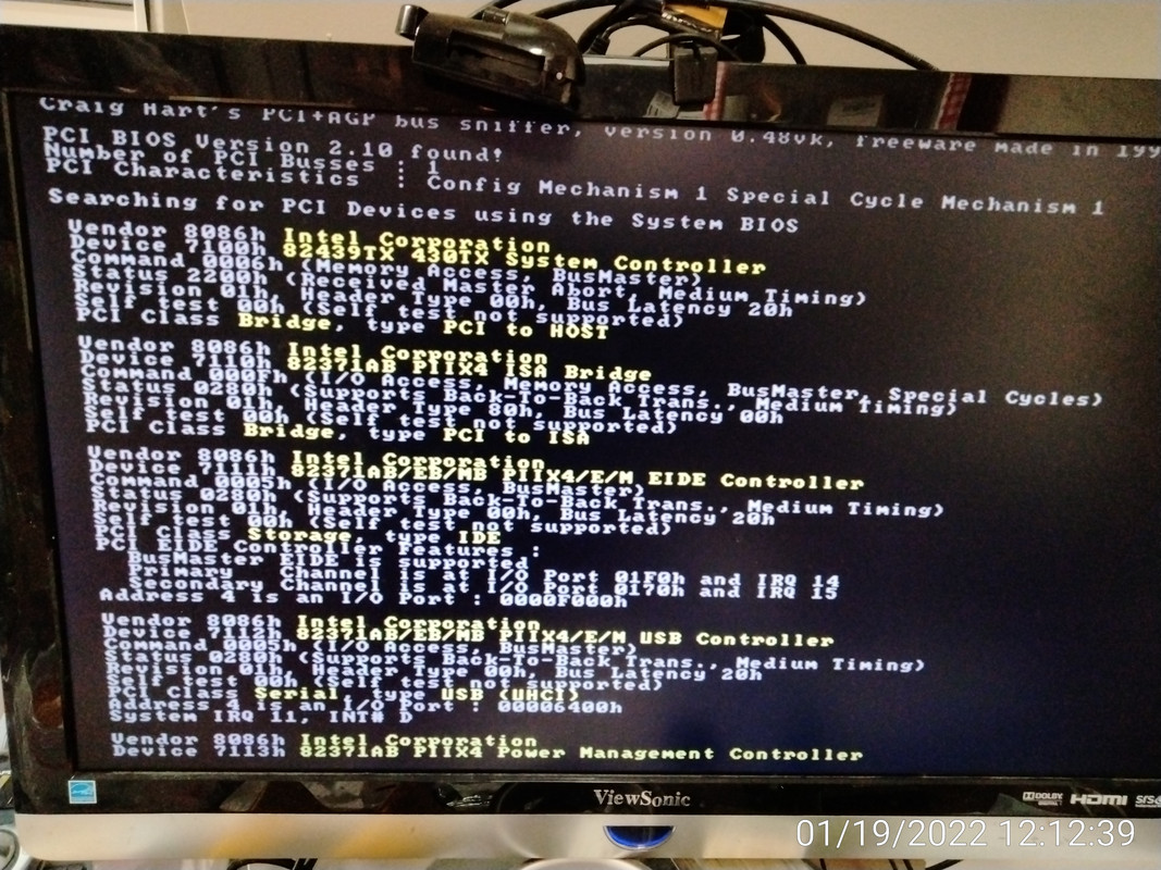
i430TX as expected. I didn't want to peel the nice label off the chipset to read it. 😀
All in all, it looks good. I have already tested it with a CF card with DOS6.22, works fine so far.
I/O, I/O,
It's off to disk I go,
With a bit and a byte
And a read and a write,
I/O, I/O