VOGONS


First post, by majestyk

User metadata
Rank Oldbie
Rank
Oldbie

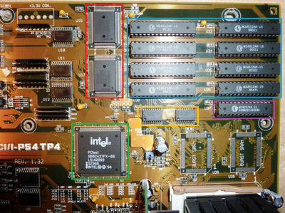
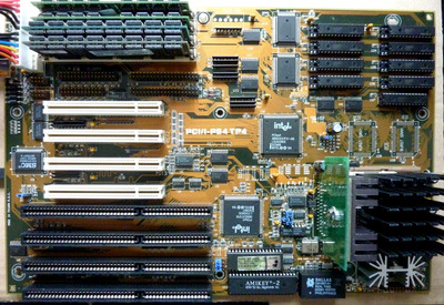
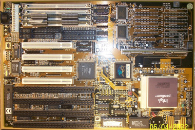
I expected this socket 5 Asus mainboard with Intel 430FX chipset to be quite troublefree, but I was wrong.

First I replaced the DALLAS RTC, added the PS2 Mouse-Connector and added the connector for a VRM module plus the necessary jumpers. With the latest BIOS (302) it detects a Pentium MMX 233 correctly (BF1 mod had to be done before of course).
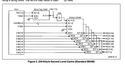
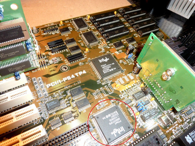
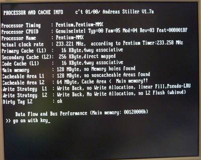
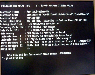
O.k., time to add some L2 cache I thought and populated the sockets first with 8 chips 32Kx8 and 8Kx8 for TAG-RAM and later with 8 chips 64Kx8 and 32Kx8 for TAG-RAM.
I also tried different sets of chips of different brands.

PCI_I_P54TP4b.JPG
Filename
PCI_I_P54TP4b.JPG
File size
810.72 KiB
Views
886 views
File license
Fair use/fair dealing exception

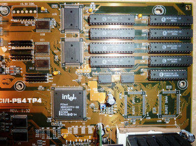
There is one jumper to select 256K or 512K on this board, but the result is always the same:
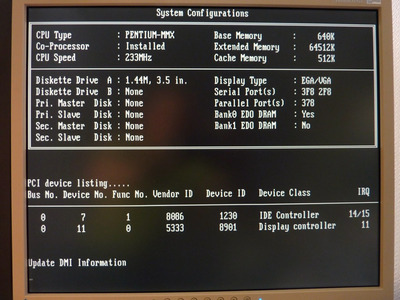
When turned on after POST the summary screen says "Cache Memory : none" and then boots into DOS fine (with no L2 cache present).
When I reset the board then, the cache size is detected correctly, but after the floppy drive has made two initial clicking noises it stops and no OS is being loaded.

l2cache detected1.JPG
Filename
l2cache detected1.JPG
File size
140.03 KiB
Views
886 views
File license
Fair use/fair dealing exception

There´s also a MR. BIOS BIOS for this board. It´s a little bit more verbose and complains with errors:
"0K Cache" and
"Cache Pattern Test Failure" after a cold start or
"Cache Address Line Test Failure" after a reset.
resulting in "External Cache n/a" at the summary screen.

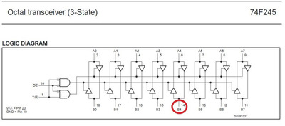
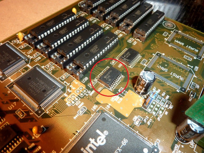
I have checked all the traces in this area carefully, also checked the pins of the northbridge, but I cannot find any visible defects.

I have had errors like this quite often, but this always used to be caused by defective (or too slow) cache chips, bad contacts, wrong size or organisation of the TAG-chip or wrong jumpering. None of this seems to apply here...

The error is NOT dependant of the frequency (FSB 33, 40, 50, 60, 66) nor of the temperature. Pressing or flexing the board has no effect either.

Reply 1 of 14, by majestyk

User metadata
Rank Oldbie
Rank
Oldbie

There were indeed some defective chips among the 256K ones. So I replaced the set with 9 chips that are 100% working in 3 other boards. The errors after a cold start ( "Cache Pattern Test Failure") are gone now, but the address line testing error persists.

So I´ll have to dig a little deeper here. First I had a look at the 430FX chipset documentation. There´s a nice diagram for a 256K L2 cache setup with 8 chips 32Kx8 and one 8kx8 Tag chip:

L2cache_wiring_FX.JPG
Filename
L2cache_wiring_FX.JPG
File size
75.94 KiB
Views
844 views
File license
Public domain
PCI_I_P54TP4ba.JPG
Filename
PCI_I_P54TP4ba.JPG
File size
889.17 KiB
Views
834 views
File license
Public domain

I first measured ALL the traces connecting the northbridge (green), Tag-RAM (violet), the two octal-bus-transceivers (orange) and the 8 SRAM sockets (blue). All connections are 100% o.k. (I/O-lines, address-lines, write enable, output enable, Vss, Vcc). The wiring between the SRAM-sockets where there are parallel lines for all or some chips is o.k. also)
(I still have to check the traces between the SRAM sockets and the 2 Intel 82438FX buffer chips (red) that connect them to the DRAM slots. But I think any problem there would probably not result in address-line errors during cache-checking.)

Since interrupted traces can be safely ruled out, there could be a faulty bus-transceiver or the northbridge itself could be defective. Because it´s the easier job by far, I´m going to replace the two 3-state bus-tranceivers (74F245) first.

Last edited by majestyk on 2022-03-01, 16:55. Edited 1 time in total.

Reply 2 of 14, by pentiumspeed

User metadata
Rank l33t
Rank
l33t

Do a diode mode check. Might find a bad pin driver or receiving pin. Red probe on ground and black on each pin in turn. You will get diode voltage drop.

Cheers,

Great Northern aka Canada.

Reply 3 of 14, by majestyk

User metadata
Rank Oldbie
Rank
Oldbie

Thanks for this tip!
I just checked all the outputs (B0:B7) of the two transceivers and there´s a diode voltage drop at all pins except for pin 14 of the left chip.

74f245.JPG
Filename
74f245.JPG
File size
39.05 KiB
Views
801 views
File license
Public domain

There are also strange results at the input side. I have ordered some 74F245 (SOIC20 package) over the weekend.

Reply 4 of 14, by majestyk

User metadata
Rank Oldbie
Rank
Oldbie

Better late than never - I finally finished this project today.
After replacing the second bus transceiver, L2 cache gets detected correctly now, the system boots with cache enabled and L2 cache is working flawlessly.
This saved me from replacing the Northbridge and/ or the two Intel buffer chips.
What a relief!

PCI_I_P54TP4_new transceiver.JPG
Filename
PCI_I_P54TP4_new transceiver.JPG
File size
258.95 KiB
Views
737 views
File license
Fair use/fair dealing exception

But the joy didn´t last long when I found out the ISA bus showed flaky behaviour. With ISA slots populated the system wouldn´t run stable. In the end I had to replace the Southbidge.

PCI_I_P54TP4_new_sb.JPG
Filename
PCI_I_P54TP4_new_sb.JPG
File size
856.76 KiB
Views
737 views
File license
Fair use/fair dealing exception

When desoldering the chips - carefully not under too much heat, no force - I found the pcb-quality, especially the stability of the traces isn´t very convincing. I had two cases of traces getting dissolved. Asus used quite a poor quality here compared to other manufacturers.

Now everything´s perfect (at least I hope...).

Reply 7 of 14, by majestyk

User metadata
Rank Oldbie
Rank
Oldbie

@flupke11: Thanks!
My usual way to remove/replace QFP chips is to first cut all pins with a Dremel using a small metal circular saw blade. I cut the pins right where they come out of the chip. After lifting the chip out the remaining parts of the pins on the soldering pads can then be removed / desoldered hasslefree (one by one or in groups) without high temperatures and without applying any force.
After some cleaning I solder the new chip the "oldschool way" with a good flux row by row.

@rasz_pl: Yes I did. But I wasn´t able to find any high resolution pictures of the pipeline burst version of the board. It seems to be quite rare. From what I found there seem to be different jumpers and capacitors / resistors populated.
I also could not be sure if the northbridge was defective before finding the underlying cause of the cache-issue. Modding the cache chips first would have complicated the troubleshooting in this case.

Reply 8 of 14, by majestyk

User metadata
Rank Oldbie
Rank
Oldbie

Today I equipped this board with 128MB RAM and did some testing. Apparently the 256 KB L2 cache is able to cache 64MB of 128MB RAM.

PCI_I_P54TP4_cache_area.JPG
Filename
PCI_I_P54TP4_cache_area.JPG
File size
161.2 KiB
Views
642 views
File license
Fair use/fair dealing exception

I also tested with 512KB L2 cache:

PCI_I_P54TP4_cache512.JPG
Filename
PCI_I_P54TP4_cache512.JPG
File size
186.32 KiB
Views
638 views
File license
Fair use/fair dealing exception

As we know Intel´s FX chipset is limited to a maximum cacheable area of 64MB RAM. I wonder why ASUS bothered to provide (and document in the manual) 32-pin SRAM sockets for 512KB L2 cache when the chipset´s maximum cacheable area is already being covered by 256K L2 cache?

Here´s finally a picture of the whole board:

PCI_I_P54TP4_total.JPG
Filename
PCI_I_P54TP4_total.JPG
File size
764.29 KiB
Views
642 views
File license
Fair use/fair dealing exception

Reply 9 of 14, by Cuttoon

User metadata
Rank Oldbie
Rank
Oldbie

You actually replaced a south bridge? That's hard core.

Does that board come with some vertically attached voltage regulator module? That's pretty ASUS. But it supports the split voltage that way? Didn't think there were FX boards that do.

majestyk wrote on 2022-04-30, 07:49:

As we know Intel´s FX chipset is limited to a maximum cacheable area of 64MB RAM. I wonder why ASUS bothered to provide (and document in the manual) 32-pin SRAM sockets for 512KB L2 cache when the chipset´s maximum cacheable area is already being covered by 256K L2 cache?

So many good reason for that.
"As we know...", well, top nerds with internet access we are, we do know that. CTCM wasn't around in 1995?

Cache was never a very exact science and so many people didn't know jack about it. German OEM Vobis was notorious for selling early 90s PCs without any installed and I have a 486 VLB motherboard that doesn't even have the sockets.
- Possibly Asus used the same layout for HX chipsets?
- Most likely: The sockets were all needed for 256 kB with 32k8 chips. If the retail customer insisted on installing 256 kB additional cache with no benefit, he'd be ASUS' guest. They're not likely to advertise limitation of their merchandise. 😉
- The option for burst SRAM has a limit for 256 kB, so there's that.

For comparison, my FX board, a Soyo 5TC0:

Soyo_5TC0.jpg
Filename
Soyo_5TC0.jpg
File size
439.95 KiB
Views
619 views
File license
Public domain

- Silkscreen for DIL SRAMs and COAST socket with 256 kB...
And it notes the 512 kB option in the manual, as well.

Soyo_5TC0_manual.png
Filename
Soyo_5TC0_manual.png
File size
63.06 KiB
Views
619 views
File license
Fair use/fair dealing exception

I like jumpers.

Reply 10 of 14, by rasz_pl

User metadata
Rank l33t
Rank
l33t
majestyk wrote on 2022-04-30, 07:49:

As we know Intel´s FX chipset is limited to a maximum cacheable area of 64MB RAM. I wonder why ASUS bothered to provide (and document in the manual) 32-pin SRAM sockets for 512KB L2 cache when the chipset´s maximum cacheable area is already being covered by 256K L2 cache?

because more cache is still better? The way I think it works is L2 is n-way associative, so the more cache installed the more potential cache slots = less collisions/evictions.

Open Source AT&T Globalyst/NCR/FIC 486-GAC-2 proprietary Cache Module reproduction

Reply 11 of 14, by pentiumspeed

User metadata
Rank l33t
Rank
l33t

All intel 430xx are 64MB cacheable limit except 430HX with dual tag sram installed can cache up to 512MB.

Cheers,

Great Northern aka Canada.

Reply 12 of 14, by majestyk

User metadata
Rank Oldbie
Rank
Oldbie

I added the header for the VRM module myself. You also have to cut some traces and add a jumperblock to enable split voltage operation.
(I also added the beeper, a socket for the Dallas RTC, the PS2 mouse-connector and replaced the 1000µF capacitors.)

All VIA chipsets of that area (Apollo family) supported at least 512MB RAM, up to 2MB L2 cache and a cacheable area of 512MB or even 1024 MB so maybe system integrators / OEMs welcomed some Intel FX based mainbords that could be promoted as "256 - 512 K L2 cache" - no matter if this really had a significant impact on performance.

The SOYO 5TC0 has a more flexible layout providing a CELP slot, supporting 3.3V and 5V (or mixed) SRAM chips with a seperate voltage regulator. And it´s prepared for a split voltage VRM also...

Reply 13 of 14, by rasz_pl

User metadata
Rank l33t
Rank
l33t

https://dependency-injection.com/intel-430fx- … riton-l2-cache/

FX was when Intel came to the conclusion buttsexing customers by gatekeeping features was a viable market strategy. This move is why we cant have nice things like ECC on the desktop anymore (ryzen might work but unofficial doesnt count).

Open Source AT&T Globalyst/NCR/FIC 486-GAC-2 proprietary Cache Module reproduction