VOGONS


Reply 20 of 44, by dionb

User metadata
Rank l33t++
Rank
l33t++
maxtherabbit wrote on 2022-04-04, 13:09:
dionb wrote on 2022-04-04, 06:04:
maxtherabbit wrote on 2022-04-03, 18:49:

Yes, intel bought the rights from Zymos

You absolutely sure of that?

I only know Zymos as a bottom-feeding chipset relabeler; just lke PC Chips later would, they just slapped their name on other peoples' silicon. I have (or had, not 100% sure if it's still here) an ISA VGA card with "Zymos Poach 51 AA" chipset, which in fact is a Trident TVGA8800CS. If they slap the exact same name on an otherwise Intel chipset, I'd be sceptical of them being the original designers...

I guess I can't say I am "absolutely" sure, but the intel branded POACH chips say copyright zymos on them, you can see for yourself in the picture in the OP

The Zymos markings are clear, but so are the Zymos markings on my TVGA8800 card, and that is definitely a regular Trident chip. I'm aware of the Wikipedia clain that the 82230/1 chipset was licensed from Zymos, but the document (Intel Processor and Peripheral Handbook) linked in Wikipedia to support that does not appear to support the claim, having a detailed description of the chipset, but no reference to Zymos that i can find.

Reply 21 of 44, by Anonymous Coward

User metadata
Rank l33t
Rank
l33t

Are you sure that it was Zymos that put the sticker on your Trident card? Maybe somebody hijacked their name.
I suppose the answer to your Zymos question is probably somewhere in the bowels of the PCmagazine archive.

"Will the highways on the internets become more few?" -Gee Dubya
V'Ger XT|Upgraded AT|Ultimate 386|Super VL/EISA 486|SMP VL/EISA Pentium

Reply 22 of 44, by dionb

User metadata
Rank l33t++
Rank
l33t++
Anonymous Coward wrote on 2022-04-05, 07:01:

Are you sure that it was Zymos that put the sticker on your Trident card? Maybe somebody hijacked their name.
I suppose the answer to your Zymos question is probably somewhere in the bowels of the PCmagazine archive.

Not just my card, they pop up every now and then:
http://old.vgamuseum.info/benchmarks/606-zymo … oach-51-aa.html

ZyMOS VGA?

Reply 23 of 44, by maxtherabbit

User metadata
Rank l33t
Rank
l33t
dionb wrote on 2022-04-05, 06:05:
maxtherabbit wrote on 2022-04-04, 13:09:
dionb wrote on 2022-04-04, 06:04:

You absolutely sure of that?

I only know Zymos as a bottom-feeding chipset relabeler; just lke PC Chips later would, they just slapped their name on other peoples' silicon. I have (or had, not 100% sure if it's still here) an ISA VGA card with "Zymos Poach 51 AA" chipset, which in fact is a Trident TVGA8800CS. If they slap the exact same name on an otherwise Intel chipset, I'd be sceptical of them being the original designers...

I guess I can't say I am "absolutely" sure, but the intel branded POACH chips say copyright zymos on them, you can see for yourself in the picture in the OP

The Zymos markings are clear, but so are the Zymos markings on my TVGA8800 card, and that is definitely a regular Trident chip. I'm aware of the Wikipedia clain that the 82230/1 chipset was licensed from Zymos, but the document (Intel Processor and Peripheral Handbook) linked in Wikipedia to support that does not appear to support the claim, having a detailed description of the chipset, but no reference to Zymos that i can find.

My thinking is this:
If you look at the zymos marked chips (like these: https://www.ultimateretro.net/en/motherboards/6702) there is no mention at all of intel. However if you look at intel marked chips, it clearly says copyright zymos. Therefore from that we can determine that zymost very clearly owns the copyright on the chip design. Whether or not they created it I cannot say, but if intel had created it and was just selling production rights to zymos, why wouldn't the situation with the markings be reversed?

Reply 24 of 44, by maxtherabbit

User metadata
Rank l33t
Rank
l33t

Top trace is MEMW#, bottom trace is ISA clock. Probed while running 3dbench2 on continuous loop

Attachments

Reply 26 of 44, by maxtherabbit

User metadata
Rank l33t
Rank
l33t

Looking at the width of the memory write strobe (~100ns) we can see that the memory writes to VRAM are working as intended and 0WS# is being properly sampled. Looking at the number of clocks between the strobes we can see many extra cycles, indicating the board applying IO recovery time.

Reply 27 of 44, by maxtherabbit

User metadata
Rank l33t
Rank
l33t

Here are some more with a 3rd probe on 0WS#

Attachments

Reply 28 of 44, by pentiumspeed

User metadata
Rank l33t
Rank
l33t

Purple waveforms has awful ringing this could mis-trigger.

See if you can insert some damping resistor in series on that one?

Cheers,

Great Northern aka Canada.

Reply 30 of 44, by bakemono

User metadata
Rank Oldbie
Rank
Oldbie

So it looks like your writes are 4 clocks apart, whereas ideally with the zerows mode it should be less than that. But at this rate you should still be getting close to 4MB/s? Unless these are only byte writes?

It seems reasonable that the designers would force a recovery time with their glue logic, at least for I/O cycles, for ISA boards that couldn't handle back-to-back cycles. I can't think of any reason it would be needed for MEM cycles though. I don't know how the 486 bus logic works but maybe whatever signal that is used to generate the wait state (or that signals the end of a bus cycle) can be traced back to one of those PAL/GAL.

again another retro game on itch: https://90soft90.itch.io/shmup-salad

Reply 31 of 44, by maxtherabbit

User metadata
Rank l33t
Rank
l33t
bakemono wrote on 2022-04-09, 13:46:

So it looks like your writes are 4 clocks apart, whereas ideally with the zerows mode it should be less than that. But at this rate you should still be getting close to 4MB/s? Unless these are only byte writes?

around 3.8MB/s yeah hmm.......

I'll move the probes over to MEMCS16# and SBHE to make sure it's actually doing 16bit cycles

bakemono wrote on 2022-04-09, 13:46:

It seems reasonable that the designers would force a recovery time with their glue logic, at least for I/O cycles, for ISA boards that couldn't handle back-to-back cycles. I can't think of any reason it would be needed for MEM cycles though. I don't know how the 486 bus logic works but maybe whatever signal that is used to generate the wait state (or that signals the end of a bus cycle) can be traced back to one of those PAL/GAL.

trying to reverse engineer a PAL/GAL is more effort than I'm willing to put into this

Reply 33 of 44, by maxtherabbit

User metadata
Rank l33t
Rank
l33t

So our quick math is indeed commensurate with what we're getting in landmark

20220409_130248.jpg
Filename
20220409_130248.jpg
File size
782.16 KiB
Views
577 views
File license
CC-BY-4.0

However the ~2MB/sec figure I was citing earlier can be seen in other benchmarks

20220409_130450.jpg
Filename
20220409_130450.jpg
File size
1.23 MiB
Views
577 views
File license
CC-BY-4.0

Reply 34 of 44, by mkarcher

User metadata
Rank l33t
Rank
l33t

One challenge of adapting the 486 bus protocol to the 286 bus protocol is that the 286 outputs the address of the next bus cycle while the data of the previous bus cycle is still happening. The address is guaranteed to be valid half a bus clock before the "official" begin of the cycle that consists of two bus clocks (with the data being transferred at the end of the second clock). So the time from the address bits being stable to the time the data needs to be on the data bits is 2.5 bus clocks, whereas such a cycle can happen every 2 bus clocks. The 486 doesn't have the concept of "forecasting" the next address, although the 386 and the Pentium processors have it as optional feature.

The 16-bit ISA specification for 0WS memory read/writes (exectly what we are after here) makes use of the 286 feature to give advance address information: The LA17-LA23 pins on the 16-bit expansion part of the ISA connector present the address bits as output by the processor with minimal delay. That means these bits are not valid during the complete bus transaction, but they are valid in advance to MEMR/MEMW. A proper 16-bit ISA memory card should use LA16-LA23 to detect whether the currently addressed 128KB block maps to this card, and assert /MEMCS16 to inform the chipset that the bus is able to perform a 16-bit cycle. The crtitical path for performing 16-bit 0WS cycles is:

  1. The bus provides the address
  2. The card assert /MEMCS16, to indicate that it is 16-bit capable, in case a memory cycle is going to happen
  3. The chipset decides whether it should perform a single 16-bit cycle or split the cycle into two 8-bit cycles and provides A0 and SBHE
  4. The chipset signals /MEMR or /MEMW
  5. The card detects that a memory cycle is indeed going to happen and asserts /0WS
  6. The chipset recognizes /0WS and terminates the cycle as soon as possible

Having the extra 0.5 clocks at the start of the cycle for detecting 16-bit capability relaxes timing constraints on this path and made 0WS cycle possible in the AT or XT286. A simple 486-to-286 bus protocol adaption implementation might want to simplify stuff by just stretching out the minimal cycle time to 3 cycles, with the whole first cycle just "forecasting" the address. This would explain one of the two extra wait states you are experiencing.

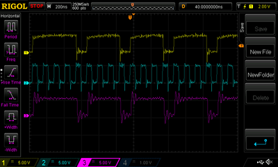
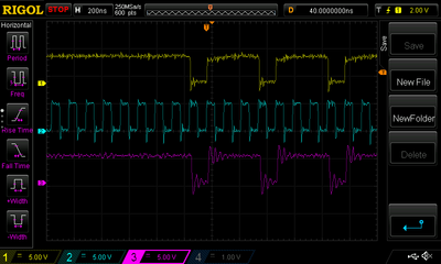
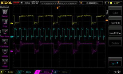
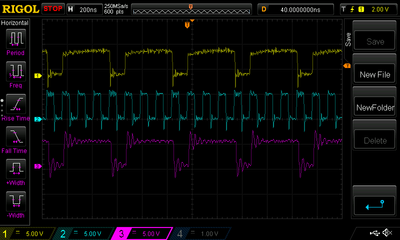
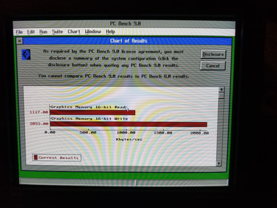
If you are after finding out exactly where the two cycles "get lost" that slow down your ISA implementation from 7.5MB/s to 3.8MB/s, you really would need to scope the 486 /ADS pin (which actually starts the cycle on the 486 side), the /MEMW pin (which indicates the write to the ISA bus) and the 486 /RDY pin (which tells the 486 that the cycle has been fully served). But knowing where the time gets lost is just to address your curiosity (if there is any), and likely you still won't be able to speed things up.

Reply 35 of 44, by mkarcher

User metadata
Rank l33t
Rank
l33t
maxtherabbit wrote on 2022-04-09, 17:05:

However the ~2MB/sec figure I was citing earlier can be seen in other benchmarks
20220409_130450.jpg

Likely, those benchmarks use 8-bit cycles to address the video card. That will drop performance by a factor of two.

Reply 36 of 44, by maxtherabbit

User metadata
Rank l33t
Rank
l33t
mkarcher wrote on 2022-04-09, 17:10:
maxtherabbit wrote on 2022-04-09, 17:05:

However the ~2MB/sec figure I was citing earlier can be seen in other benchmarks
20220409_130450.jpg

Likely, those benchmarks use 8-bit cycles to address the video card. That will drop performance by a factor of two.

I don't think so. (This was with the 24MHz ISA oscillator FYI)

20220127_193709.jpg
Filename
20220127_193709.jpg
File size
1.92 MiB
Views
547 views
File license
CC-BY-4.0

Reply 37 of 44, by mkarcher

User metadata
Rank l33t
Rank
l33t
maxtherabbit wrote on 2022-04-09, 19:52:
mkarcher wrote on 2022-04-09, 17:10:
maxtherabbit wrote on 2022-04-09, 17:05:

However the ~2MB/sec figure I was citing earlier can be seen in other benchmarks
20220409_130450.jpg

Likely, those benchmarks use 8-bit cycles to address the video card. That will drop performance by a factor of two.

I don't think so. (This was with the 24MHz ISA oscillator FYI)
20220127_193709.jpg

Oh, I see. The main difference I notice is that the display of PC Bench seems to be in 16-color graphics mode, whereas Landmark is in text mode. The memory organization of 16-color modes and Mode X makes it difficult for a graphics card to execute 16-bit cycles in one transaction, so a lot of graphics cards (I don't know about ET4000-based cards, though) do not assert /MEMCS16 if they are in 16-color modes or Mode X. If the measurement by PC Bench is performed while the graphics card is in 16-color mode, whereas the measurement by landmark is performed while the card is in text mode, that might explain the difference.

Reply 38 of 44, by Deunan

User metadata
Rank Oldbie
Rank
Oldbie

I'd like to add a few techical bits that are perhaps worth considering. The 386 has a NA# signal that allows for limited bus pipelining - it can drive a full set of control signals (not just the address) 1 bus cycle (2 clock cycles) earlier to allow the chipset to do things like cache tag checks or perhaps address output if 2 or more RAM banks are used. Though frankly it's rather difficult to do properly and I have not seen it used (but then again I have not probed each and every mobo I have).

The 486 doesn't have NA#, it solves most of the bus pressure problem with its internal cache and burst transfer to fill cache lines. This is way easier to support since all the 16 bytes are consecutive addresses. However, the cache presents certain problems which Intel docs are pointing out: Unlike on 386 you can't do a short jump to next instruction to make sure there's going to be a memory read (instruction fetch in this case) between each I/O access. That jump and read can be filled from cache on 486 with no extra bus cycles. What's worse, a single OUT will not be buffered by the CPU but consecutive ones will be (starting from 2nd). This is because unlike on 386 there are now 4 write buffers on-chip which can store data before it's actually output to the bus. In fact the 486 can even re-order a read in front of the writes (but not I/O writes) in certain cases so you are not guaranteed the actual bus order - this however should not affect memory space between 640k and 1M, since most chipsets will not drive KEN# to the CPU for this region and thus not allow it to be cached. With certain exceptions maybe, ones that can be enabled/disabled in the BIOS settings (like BIOS ROM and video card ROM address space for example).

So the extra cycle on I/O might be a cheap (in terms of logic needed, not performance) way to allow recocery, to ensure code written for slow cards (that worked on 386 and below) would also work on 486. Any extra memory waitstates to what is usually ISA space might be a similar workaround - either because it's already done for I/O and the logic is there, or because there are some potential problems there too and this is the easiest way to deal with them. I can't think of any particular reason why memory on ISA card would not allow back to back transfers (and there is a ready signal as well) but I also never made my own 486 based system and chipset - perhaps there are cases, or just particular cards, that can't deal with it.

Reply 39 of 44, by maxtherabbit

User metadata
Rank l33t
Rank
l33t

my best guess is they just couldn't be bothered to implement different bus timing logic for memory and I/O transactions, either due to laziness, cowardice, or both