Reply 1 of 21, by Anonymous Coward

Rank
l33t
- Rank
- l33t
SLC/e should be 5V right? The fastest QFP100 CPU at 5V is the TI486SXLC-40 (some people have had success with the 3.3V 50MHz part too). Some boards also don't like the SXLC.
In my opinion upgrading your CPU won't be worth the trouble. You might be able to get an extra 20% CPU power.
I think your best bet would be to try changing the oscillator to see if your CPU can overclock to 40MHz. Heatsink and fan are probably a good idea if you want to go that route.
"Will the highways on the internets become more few?" -Gee Dubya
V'Ger XT|Upgraded AT|Ultimate 386|Super VL/EISA 486|SMP VL/EISA Pentium
Reply 2 of 21, by TimWolf
Rank
Member
Anonymous Coward wrote on 2022-04-14, 03:30:SLC/e should be 5V right? The fastest QFP100 CPU at 5V is the TI486SXLC-40 (some people have had success with the 3.3V 50MHz part too). Some boards also don't like the SXLC.
In my opinion upgrading your CPU won't be worth the trouble. You might be able to get an extra 20% CPU power.
I think your best bet would be to try changing the oscillator to see if your CPU can overclock to 40MHz. Heatsink and fan are probably a good idea if you want to go that route.
The primary desire is to get the 8kb cache from the TI chip. This Cx486SLC/e-33MP is 3.3v with 1kb cache. The intended 50mhz TI is also 3.3v but 8kb cache. My primary goal is to find a board to run the cpu more than to upgrade the motherboard. I'm just trying to decide on a good (cheap) candidate to play doctor with before I start.
Reply 3 of 21, by jesolo

Rank
l33t
- Rank
- l33t
Based on benchmarks I've seen of the 486DLC vs 486SXL CPU's (which have a 32-bit external data bus), the difference was negligible.
I think that the external 16-bit data bus on your motherboard is more of a limiting factor than the 1KB L1 vs 8KB L1 cache.
Reply 4 of 21, by Deunan
Rank
Oldbie
IMO the upgrade to 8k cache is not worth the trouble, unless it's a "project" - that is, it's more about trying to do it rather then expecting a decent performance boost. The sad truth is internal cache in these DLC-type CPUs is not all that fast (mostly due to rather narrow 32-bit bus). Plus you can't be sure the new CPU clock, which would also affect the CPU to chipset bus speed, will actually work properly in this mobo.
What could make it worthwhile is 66MHz SXLC, since it has clock doubler (even if that would require running a configuration tool on boot). The problem is there aren't, AFAIK, 5V variants of the 66MHz SXLC. In fact even finding the 66MHz part is rather difficult, and I have seen some poorly done fakes already.
Reply 5 of 21, by Anonymous Coward
Rank
l33t
- Rank
- l33t
How do you know if the 66MHz SXLC2 is fake or not?
"Will the highways on the internets become more few?" -Gee Dubya
V'Ger XT|Upgraded AT|Ultimate 386|Super VL/EISA 486|SMP VL/EISA Pentium
Reply 6 of 21, by Deunan
Rank
Oldbie
I can't find that ebay listing now but the chip looked odd. All 386SX-class CPUs come in the PQFP-100 package with those wings at the corners. This one didn't have them.
Reply 7 of 21, by mkarcher
Rank
l33t
jesolo wrote on 2022-04-14, 06:24:Based on benchmarks I've seen of the 486DLC vs 486SXL CPU's (which have a 32-bit external data bus), the difference was negligible.
I think that the external 16-bit data bus on your motherboard is more of a limiting factor than the 1KB L1 vs 8KB L1 cache.
This point sounds strange to me. The 16-bit bus on the 486SLC is actually the main bottleneck of the processor. So everything that takes load from that bottleneck is going to be a big win. The 1KB L1 cache of the Cyrix SLC processor is little more than a joke, but very useful to cache tight benchmark loops and achieve high, 486-like scores in Norton SI. The 8KB cache of the TI part would be able to cache a lot more of relevant DOS use-cases. So The 1KB vs. 8KB L1 cache is a win because of the grossly undersized bus interface.
Don't put too much hope into the clock doubler (50MHz instead of 25MHz) though, because as soon as you miss the L1 cache, waiting for the external bus with 50MHz clocking just uses more power but doesn't gain any speed. The official Cyrix performance scores (claimed to be based on PCBench 8.0) are quite revealing about the non-effectiveness of the clock doubling (although at just 1KB L1):
- Cx486SLC-25: 36 points
- Cx486SLC-33: 39 points
- Cx486SLC-50: 40 points
So increasing the clock from 25 to 50 MHz (+100%) at a measely one KB of L1 just improves the score by around 11%, and you can reach nearly the improvement by just increasing the FSB by 33%.
Reply 8 of 21, by Anonymous Coward
Rank
l33t
- Rank
- l33t
Deunan wrote on 2022-04-14, 17:12:I can't find that ebay listing now but the chip looked odd. All 386SX-class CPUs come in the PQFP-100 package with those wings at the corners. This one didn't have them.
Not having the "wings" doesn't make them fake. It's been a while since I looked in the SXL databook, but I believe that it's a legitimate package type. I'm pretty sure if you look at the evergreen interposers that use the SXL2 and SXLC2 chips, you will find they also don't have wings.
"Will the highways on the internets become more few?" -Gee Dubya
V'Ger XT|Upgraded AT|Ultimate 386|Super VL/EISA 486|SMP VL/EISA Pentium
Reply 9 of 21, by rmay635703
Rank
Oldbie
- Rank
- Oldbie
Time to solder in an IBM SLC2, now your playing with power
Reply 10 of 21, by Anonymous Coward
Rank
l33t
- Rank
- l33t
Soldering in an IBM SLC sounds like a good idea, but unless the board was designed to accept one how will it flush the cache?
"Will the highways on the internets become more few?" -Gee Dubya
V'Ger XT|Upgraded AT|Ultimate 386|Super VL/EISA 486|SMP VL/EISA Pentium
Reply 11 of 21, by TimWolf
Rank
Member
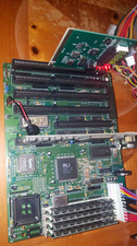
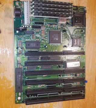
Here is a picture of one of the 8517 v3.3 Ali M1217-40 board that I plan to play doctor on (From a user "Horun" vogons post). It does have the 1kb cache on the cpu (on my board), and the current cpu is a 3.3v. I don't have the board yet, but as it has 1kb cache on the cpu, hopefully the bios has the cache options built in. If not I'll try it with software as shown in the Cpu galaxy video. I plan to add on the Texas Instruments TI486SXLC2-G50-PQ (8k 3.3v) and a Green 4C87SLC-40 FPU. Sadly no on motherboard cache, so that is a down side but I can't complain for $35 shipped. I just want to play with the TI486SXLC2-G50-PQ and see what I can do with it.
This build while it may not be as fast in the end, I hope it works, was inspired by watching:
https://www.youtube.com/watch?v=40TT2bBQ0bc&t
Reply 12 of 21, by Anonymous Coward
Rank
l33t
- Rank
- l33t
SLC/e should be a 5V part with power management. I think the SLC/e-V is the 3.3V version.
There are some 386SX boards that support voltage regulation (other than the IBM made ones), but they came out pretty late and are quite rare.
"Will the highways on the internets become more few?" -Gee Dubya
V'Ger XT|Upgraded AT|Ultimate 386|Super VL/EISA 486|SMP VL/EISA Pentium
Reply 13 of 21, by TimWolf
Rank
Member
Anonymous Coward wrote on 2022-04-15, 03:37:SLC/e should be a 5V part with power management. I think the SLC/e-V is the 3.3V version.
There are some 386SX boards that support voltage regulation (other than the IBM made ones), but they came out pretty late and are quite rare.
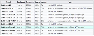
I was going off this Wikipedia chart. it wouldn't be the first time a Wikipedia page was wrong.
Attachments
Reply 14 of 21, by Anonymous Coward
Rank
l33t
- Rank
- l33t
That clearly looks like an error, as all other speed grades of that type are 5V.
According to the SLC databook, the 3.3V parts can also operate at 5V, but at 3.3V they only consume about 30% as much power. You should still be able to operate the -G50 at 5V as long as it has adequate cooling.
"Will the highways on the internets become more few?" -Gee Dubya
V'Ger XT|Upgraded AT|Ultimate 386|Super VL/EISA 486|SMP VL/EISA Pentium
Reply 15 of 21, by mkarcher
Rank
l33t
TimWolf wrote on 2022-04-15, 03:55:Anonymous Coward wrote on 2022-04-15, 03:37:SLC/e should be a 5V part with power management. I think the SLC/e-V is the 3.3V version.
There are some 386SX boards that support voltage regulation (other than the IBM made ones), but they came out pretty late and are quite rare.
I was going off this Wikipedia chart. it wouldn't be the first time a Wikipedia page was wrong.
There is another mistake in that table. I had a laptop based on the 486SLC2 (the clock-doubling doesn't really make sense to me with the small L1 cache and the 16-bit non-burst bus interface), and I can confirm that this processor does have advanced power management support, even without having an "e" in the model number. It looks like Cyrix omitted the "e" due to limited space for markings. I failed to find any official datasheets on that processor, though, so I don't have a wikipeda-worthy reliable source on that claim.
Reply 16 of 21, by Deunan
Rank
Oldbie
I don't have any Cyrix SLC2 chips so I have no idea how much performance the clock doubler provides with limited 1k cache. Probably not much. But there is a point toi using clock doubler on TI SXLC(2) - sure, it won't be x2 gain, or even close to it, but we are talking about replacing the soldered CPU here. There will be hard limits to what can be achieved, if one needs a faster system then the only way is full 32-bit bus, or perferably a 486DX(2) system.
These are benchmark results from my own system, in which I replaced 5V 386SX with 3V3 SXLC - these chips apparently use the same manufacturing process and seem to survive 5V power, but yes they do run hot. All Cyrix/Ti replacement pull more power anyway, and would benefit from at least a heatsink (which I did put on my chip, with the help of double-sided thermal transfer sticky tape). BTW this was originally 33MHz system but I downgraded it to 25MHz exactly because I wanted to try the clock doubler in my G50 part.
TI 486SXLC2 25MHz:
* NSSI (/SAFE):
12780 Dhry/s (fi 12845, 16-bit code)
3155 kWhet/s (fi 3167, real mode)
* SI 8.0:
40.7
* Speedsys 4.78:
12.65
-- Trident TVGA8900D (1024k x32):
* TOPBENCH:
82
* Speedsys 4.78 VESA mem:
2585 kB/s
* 3DBench (1.0, 1.0c):
14.7, 14.6
* PC Player Benchmark (320, 640):
3.6, N/A
* Landmark 6.00:
104 MHz AT, N/A, 3101.07 chr/ms
* Doom (low, high):
2134/3089, 2134/10955
TI 486SXLC2 50MHz (2x25):
* NSSI (/SAFE):
20085 Dhry/s (fi 20154, 16-bit code)
3279 kWhet/s (fi 3291, real mode)
* SI 8.0:
73.6
* Speedsys 4.78:
22.19
-- Trident TVGA8900D (1024k x32):
* TOPBENCH:
111
* Speedsys 4.78 VESA mem:
2586 kB/s
* 3DBench (1.0, 1.0c):
22.2, 21.8
* PC Player Benchmark (320, 640):
5.5, N/A
* Landmark 6.00:
203 MHz AT, N/A, 3101.07 chr/ms
* Doom (low, high):
2134/2281, 2134/7960
One of these days I'll do a test run with the original clock generator at 33MHz to see if Doom would benefit more from faster CPU clock or perhaps faster memory bus. But there is some benefit to the clock doubler.
Reply 17 of 21, by mkarcher
Rank
l33t
Deunan wrote on 2022-04-15, 09:18:I don't have any Cyrix SLC2 chips so I have no idea how much performance the clock doubler provides with limited 1k cache. Probably not much. But there is a point toi using clock doubler on TI SXLC(2) .
One of these days I'll do a test run with the original clock generator at 33MHz to see if Doom would benefit more from faster CPU clock or perhaps faster memory bus. But there is some benefit to the clock doubler.
Looking at your benchmarks (the application benchmarks like Doom or 3DBench), I fully agree with the clock doubler on the SXLC being worth it. You get around 50% improvement in 3DBench and the PC Player benchmark, and still around 35% improvement in Doom. While that's not the raw 100% improvement you experience in some of the synthetic benchmarks, its very likely more than the 33% clock advantage 33MHz compared to 25MHz will be able to deliver. It seems the code of the core loops of the 3D applications fits nicely into the 8KB L1 cache, and it's likely just the texture data that causes cache misses.
Reply 18 of 21, by TimWolf
Rank
Member
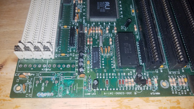
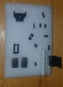
The board arrived. A bunch of barrel battery acid damage. Cleaned off the bubbled mask, tinned everything affected, fixed three traces. Green nail polish over that. Added a crystal socket and vertical cr2032 battery holder. Works like a champ but no further testing yet.
Attachments
Reply 19 of 21, by TimWolf
Rank
Member
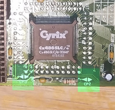
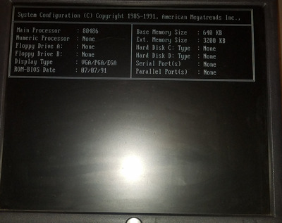
Does anyone happen to have the manual for the 8517 v3.3 Ali 1217 Motherboard either online or that they could scan? I've looked everywhere I can think, and the closest was a youtuber that showed the cover in their video but didn't open it. I am trying to find out the functions of CP2 and CP3, bridgeable points on the board. in one of their videos they mention that one of those is to enable the on chip cache. Also, how would I go about confirming that the chip that I have on here Cx486SLC/e-33MP is a 5v chip? Since the resources online say otherwise, and I don't want to kill the SXLC2. I had hoped there may be a way to change the voltage built in the board as it is so advanced for a 386. Or maybe add a little inverter circuit.
Thanks in advance!
~TW