VOGONS


First post, by Tronix

User metadata
Rank Member
Rank
Member

Hello,
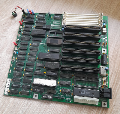
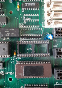
I recently got this motherboard (photo by seller):

ezgif.com-gif-maker.jpg
Filename
ezgif.com-gif-maker.jpg
File size
1.36 MiB
Views
1089 views
File license
Public domain

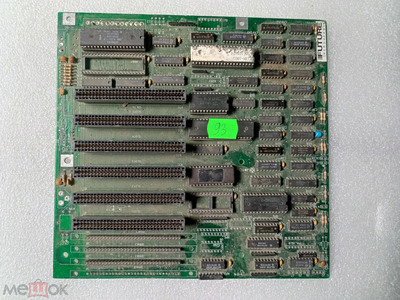
I identified the board as Jaton JXM-1003 aka JXM-JET 88-V2 and found some jumper info here: Re: 8088/XT Clone Motherboard - Keyboard Not Working
As you can see, the board is missing: power connector, keyboard connector, tantalums, resistors in some places, quartz and crystal oscillator, trimmer capacitor, i8284, i8288, dip-switch, PLS connectors for connecting LEDs/jumpers, one slot for sipp module, delay line . And the most important component - PAL16L8.

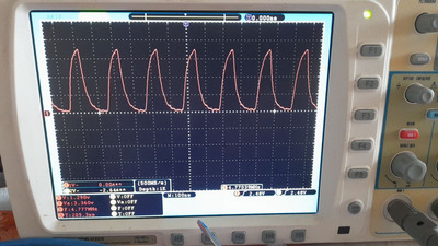
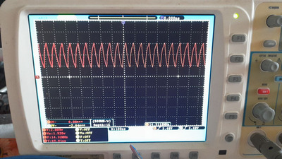
So, i restored power and keyboard connectors, installed i8284, crystal and crystal generator and fixed OSC and CLK clocks

photo_2022-07-26_14-35-39.jpg
Filename
photo_2022-07-26_14-35-39.jpg
File size
163.11 KiB
Views
1089 views
File license
Public domain
photo_2022-07-26_14-35-16.jpg
Filename
photo_2022-07-26_14-35-16.jpg
File size
163.75 KiB
Views
1089 views
File license
Public domain

Then i put the socket and stuck the i8288 bus arbiter, along the way restoring several tracks above and below it;
Fixed RESET by soldering all sorts of diodes / capacitors in the J4-J3 area;
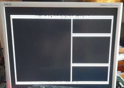
Burn in 2764 EEPROM Landmark Diagnostic ROM, started the board with CGA card and got first signs of life:

photo_2022-07-26_16-27-28.jpg
Filename
photo_2022-07-26_16-27-28.jpg
File size
154.68 KiB
Views
1089 views
File license
Public domain

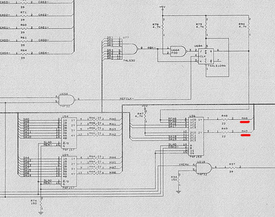
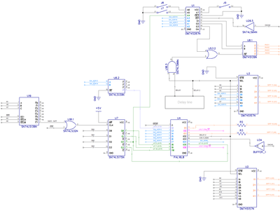
Encouraged by the success, I replaced the SIPP holders with SIMM30 holders and approached the main problem - the lack of PAL16L8. Using a multimeter, I tried to draw a section of the circuit around PAL16L8 :

pal_schm8.png
Filename
pal_schm8.png
File size
49.8 KiB
Views
1089 views
File license
Public domain

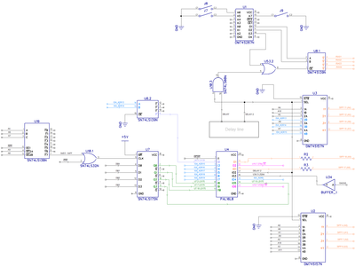
I tried to write this equations for PLD logic:

"INPUT PINS
!MEMR PIN 1;
!A13_A14 PIN 2;
A15,A16,A17,A18,A19 PIN 3,4,5,6,7;
D0,D1,D2,D3 PIN 8,9,11,14;
A8 PIN 15;
DACK PIN 16;
MPX PIN 17;

"OUTPUT PINS
!CS1,!CS2 PIN 12,13;
MA8,MA9 PIN 18,19;

EQUATIONS
CS1 = A19 & A18 & A17 & A16 & A15 & A13_A14 & MEMR & DACK;
CS2 = A19 & A18 & A17 & A16 & A15 & (!A13_A14) & MEMR & DACK;

WHEN (MPX) THEN
MA8 = (A16 & DACK) # (A17 & !DACK);
ELSE
MA8 = A8;

WHEN (MPX) THEN
MA9 = (A18 & DACK) # (A19 & !DACK);
ELSE
MA9 = 1;

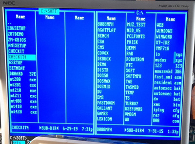
This allowed the system to boot DOS 5.0 from XT-IDE, but almost no applications run. Doesn't start Volcov Commander, CheckIt, Cats game etc... I'm not sure that I correctly described the logic of the PLD, so I ask for your help.

https://github.com/Tronix286/

Reply 1 of 15, by SSTV2

User metadata
Rank Oldbie
Rank
Oldbie

I see that you are investing a good amount of time restoring that MB and probably are having a whale of time doing so 😀. That PAL chip is going to be a tough nut to crack here, but I see that you are willing to tackle it instead of seeking an image dump from someone, thus i'll try give my two cents (though I'm not an expert on IBM PCs/XTs by any means).

Lets assume that memory map is as follows:

FE000 - FFFFF 8KB BIOS ROM
F6000 - FDFFF 32KB BASIC ROM

ADDR reqd. for BIOS ROM (8KB) CS1 generation would be - FE000-FFFFF = 1111 1(11)X (A19 A18 A17 A16 A15 A14 A13 unused), value in parentheses is a combination of A13 and A14, that goes through 74139, when both inputs are HIGH, output at pin 9 of 74139 is LOW, otherwise it's always HIGH.

ADDR reqd. for BASIC ROM (4x8KB) CS2 generation would be - F6000-FDFFF = 1111 0(11)X or 1111 1(00)X or 1111 1(01)X or 1111 1(10)X.

Operators:

& - AND
# - OR
! - NOT

EQs:

CS1 = A19 & A18 & A17 & A16 & A15 & !A13_A14 & !MEMR

CS2 = A19 & A18 & A17 & A16 & !A15 & !A13_A14 & !MEMR # A19 & A18 & A17 & A16 & A15 & A13_A14 & !MEMR

DACK0 is used in RAM refresh circuitry, it's not needed here.

Now address selection and RAS generation are a bit unclear to me, also I don't get that CPLD syntax with conditions, could you rewrite it in WinCUPL way and explain why you implemented such equations?

By the way, are you sure there's an Addr.8 line at pin 15 instead of /MEMW?

Reply 2 of 15, by Tronix

User metadata
Rank Member
Rank
Member

Thanks for your answering, SSTV2!

SSTV2 wrote on 2022-08-02, 02:24:

Lets assume that memory map is as follows:

FE000 - FFFFF 8KB BIOS ROM
F6000 - FDFFF 32KB BASIC ROM

That's right! For some reason I thought that FE000 - FFFFF 8K BIOS ROM and F8000 - FFFFF 32K BIOS ROM. I forgot about BASIC and thought it was just two different types of BIOS ROM 😀 I will redo the conditions for choosing a /CS's as you advise, thanks!

SSTV2 wrote on 2022-08-02, 02:24:

DACK0 is used in RAM refresh circuitry, it's not needed here.

Yes, DACK0 ~= /REFRESH, so when DACK0 active - this is NOT a refresh cycle and we can safely set the active level to the /OE pin on EEPROM. Otherwise, when DACK = 0, this is refresh cycle and we do not need output data from EEPROMs. I argued something like this. Anyway, I tried to remove the DACK from the CS's select expressions and it did not affect anything....

SSTV2 wrote on 2022-08-02, 02:24:

Now address selection and RAS generation are a bit unclear to me, also I don't get that CPLD syntax with conditions, could you rewrite it in WinCUPL way and explain why you implemented such equations?

Iam using ABEL dialect for PLD, this is great-grandfather modern HDL languages, it is slightly more high-level than simple boolean expressions. But of course, in the end it all comes down to them.
Why iam implemented such equations? So, i looked through the available circuits of XT computers and found in one of them a node that seemed to me similar to the signal generation MA8 MA9:

mpx.JPG
Filename
mpx.JPG
File size
367.57 KiB
Views
1043 views
File license
Public domain

As I roughly understood, from the diagram it follows that:
if MPX (SLAD) = 0, !DACK = 0 then A8 = A8;
if MPX (SLAD) = 0, !DACK = 1 then A8 = A8;
if MPX (SLAD) = 1, !DACK = 0 then A8 = A16;
if MPX (SLAD) = 1, !DACK = 1 then A8 = A17;
This is what I tried to encode in the GAL... As it turned out, this was not true (see below).

SSTV2 wrote on 2022-08-02, 02:24:

By the way, are you sure there's an Addr.8 line at pin 15 instead of /MEMW?

I checked twice, pin 15 going to ISA bus Addr.8 signal.

And now to the good news 😀
I managed to start the system with such expressions (the /CS choice has not yet been redone):

"INPUT PINS
!MEMR PIN 1;
!A13_A14 PIN 2;
A15,A16,A17,A18,A19 PIN 3,4,5,6,7;
D0,D1,D2,D3 PIN 8,9,11,14;
A8 PIN 15;
DACK PIN 16;
MPX PIN 17;

"OUTPUT PINS
!CS1,!CS2 PIN 12,13;
MA8,MA9 PIN 18,19;

EQUATIONS

CS1 = A19 & A18 & A17 & A16 & A15 & A13_A14 & MEMR & DACK;
CS2 = A19 & A18 & A17 & A16 & A15 & (!A13_A14) & MEMR & DACK;

WHEN (MPX) THEN
MA8 = A17;
ELSE
MA8 = A16;

WHEN (MPX) THEN
MA9 = A19;
ELSE
MA9 = A18;

or in simple boolean conditions:

CS1     = !(  !MEMR & !A13_A14 & A15 & A16 & A17 & A18 & A19 & DACK );

CS2 = !( !MEMR & A13_A14 & A15 & A16 & A17 & A18 & A19 & DACK );

MA8 = !( !A17 & MPX
# !A16 & !MPX );

MA9 = !( !A19 & MPX
# !A18 & !MPX );

This allowed me to boot into DOS, run a memory test in CheckIt, play Commander Keen 5. Like everything is working properly.

photo_2022-08-01_19-24-39.jpg
Filename
photo_2022-08-01_19-24-39.jpg
File size
199.98 KiB
Views
1043 views
File license
Public domain

Booted with two SIMM of 256kb each, which gave a total of 512kb of memory. I also booted with four SIMM of 256kb each, which gave a total of 640kb of memory. But the configuration with three 256Kb SIMM shows some strange number, something like about 576kb of memory, that is, it takes one of the bars for 64kb. When closing J8 and starting with three strips of 256kb each, it turns out 640kb main and another 64kb window in E000-F000 (umb). And when you close J7 and start with three strips of 256kb each, you get 640kb of the main one.

It remains a mystery why, then, the ISA_A8 signal (15 pins) was put into the PAL at all, and also what the D0..D3 bits coming from port 0xE0 could control. But apparently this will remain a mystery.

20220802_085659.jpg
Filename
20220802_085659.jpg
File size
1.55 MiB
Views
1043 views
File license
Public domain

https://github.com/Tronix286/

Reply 3 of 15, by weedeewee

User metadata
Rank l33t
Rank
l33t

Amazing work Tronix !

I was looking at the photo of the board and the photo of the board in the other vogons thread and was wondering
What use have U6, RP5 and U9 since they still seem to be missing on the photo of your board, while present on the photo of the other thread.

Right to repair is fundamental. You own it, you're allowed to fix it.
How To Ask Questions The Smart Way
Do not ask Why !
https://www.vogonswiki.com/index.php/Serial_port

Reply 4 of 15, by Tronix

User metadata
Rank Member
Rank
Member
weedeewee wrote on 2022-08-02, 08:34:

Amazing work Tronix !

Thanks.

weedeewee wrote on 2022-08-02, 08:34:

I was looking at the photo of the board and the photo of the board in the other vogons thread and was wondering
What use have U6, RP5 and U9 since they still seem to be missing on the photo of your board, while present on the photo of the other thread.

I don't know for sure, probably just slightly different versions of the boards. U6 is 74S280 - Parity Generators/Checker and U5 - 74LS245 buffer between SIPP data bus and internal motherboard data bus. On my version of the board, the traces between the 74LS245 buffer inputs and its outputs are closed, so if you install a IC, you must first cut all eight traces between the inputs pins and outputs pins.

photo_2022-08-02_15-51-10.jpg
Filename
photo_2022-08-02_15-51-10.jpg
File size
177.42 KiB
Views
1009 views
File license
Public domain

Perhaps my version of the board does not support parity, or perhaps it is implemented somehow differently on small logic. In any case, I don't think I'll ever run into parity errors, so I won't tamper with this schematic node.

https://github.com/Tronix286/

Reply 5 of 15, by PTherapist

User metadata
Rank Oldbie
Rank
Oldbie
Tronix wrote on 2022-08-02, 07:09:

Booted with two SIMM of 256kb each, which gave a total of 512kb of memory. I also booted with four SIMM of 256kb each, which gave a total of 640kb of memory. But the configuration with three 256Kb SIMM shows some strange number, something like about 576kb of memory, that is, it takes one of the bars for 64kb. When closing J8 and starting with three strips of 256kb each, it turns out 640kb main and another 64kb window in E000-F000 (umb). And when you close J7 and start with three strips of 256kb each, you get 640kb of the main one.

When you had 4x 256K chips installed, did the boot memory test mention the remaining 384K at all (might be certain BIOS version specific)? I have this same motherboard and with the 4 chips it shows 640KB + "384KB Virtual" at boot.

Reply 6 of 15, by Tronix

User metadata
Rank Member
Rank
Member
PTherapist wrote on 2022-08-02, 13:13:

When you had 4x 256K chips installed, did the boot memory test mention the remaining 384K at all (might be certain BIOS version specific)? I have this same motherboard and with the 4 chips it shows 640KB + "384KB Virtual" at boot.

No, i don't see "384KB Virtual" at boot screen. I dumped bios from EEPROM and will attach it to the message, but I did not find the "virtual" text string in it.

UPD: I found your post with your BIOS dump here Re: JATON JXM-10MHZ-V3, XT motherboard ,
so bios'es are different. Your BIOS have Phoenix copyright and string "Virtual RAM: ". My BIOS dos't have "virtual" string and marked as "T U R B O - X T 1989"...

UPD2: PTherapist, no chance to read/dump PAL in any way?

Attachments

  • Filename
    jaton_xt.zip
    File size
    6.13 KiB
    Downloads
    37 downloads
    File license
    Public domain

https://github.com/Tronix286/

Reply 7 of 15, by PTherapist

User metadata
Rank Oldbie
Rank
Oldbie
Tronix wrote on 2022-08-02, 13:23:

UPD2: PTherapist, no chance to read/dump PAL in any way?

All I have here is a MiniPro. Can this read PAL chips, as I don't see anything listed in the program?

Edit: nevermind, I see it requires the building of an adapter. A bit out of my league at present I'm afraid.

Reply 8 of 15, by Tronix

User metadata
Rank Member
Rank
Member
PTherapist wrote on 2022-08-02, 14:24:

Can this read PAL chips, as I don't see anything listed in the program?

I don't know, probably not. Thanks anyway.

https://github.com/Tronix286/

Reply 9 of 15, by SSTV2

User metadata
Rank Oldbie
Rank
Oldbie

Great job!

The whole picture is much clearer with that schematic at hand, based on it and 74f153 multiplexer chip, I think the generation of addr.8 and addr.9 signals or RAM should look like this:

A8 = DACK & !SLAD & A16 
# DACK & SLAD & A17
# !DACK & !SLAD & A8
# !DACK & SLAD & A8

A9 = DACK & !SLAD & A18
# DACK & SLAD & A19
# !DACK & !SLAD <-
# !DACK & SLAD <- these two lines probably can be ignored

*Here SLAD is address selection (LOW=lower bits, HIGH=higher bits), it originates from delay line i presume.

And, of course, when these conditions are not met, A8/A9 are at low logic levels.

Now that data latch is a complete mystery to me also, but it somehow should affect PAL's outputs.

PS. That is one great schematic collection, wish I knew about that book earlier 😁

Reply 10 of 15, by Tronix

User metadata
Rank Member
Rank
Member
SSTV2 wrote on 2022-08-02, 14:53:

Great job!

I think the generation of addr.8 and addr.9 signals or RAM should look like this:
...skip...

Thank you. In accordance with this scheme (from scaned paper book), yes, it should look something like this, and I did something like this before, but this did not allow any programs to load. But I will try to apply exactly your equationss for the experiment. Now i made your corrections to the /CS selecting code, everything works fine. Now my firmware looks like this:

CS1     = !(  !MEMR & !A13_A14 & A15 & A16 & A17 & A18 & A19 );

CS2 = !( !MEMR & A13_A14 & A15 & A16 & A17 & A18 & A19
# !MEMR & !A13_A14 & !A15 & A16 & A17 & A18 & A19 );

MA8 = !( !A17 & MPX
# !A16 & !MPX );

MA9 = !( !A19 & MPX
# !A18 & !MPX );

So far everything is working great.

SSTV2 wrote on 2022-08-02, 14:53:

Now that data latch is a complete mystery to me also, but it somehow should affect PAL's outputs.

Yes, the board also has U1 DM74S287 PROM 256x4 memory, whitch generating /RAS signals. One of bit (D2) from latch enters not only PAL, but also goes directly to address A4 of that PROM. I update circuit with this traces:

pal_schm9.png
Filename
pal_schm9.png
File size
52.93 KiB
Views
939 views
File license
Public domain

I can desolder this PROM and read its contents, but I'm not sure if this is necessary. Perhaps all this was done for the sake of some support for EMS memory of some early revision, but we are unlikely to find the original software.

SSTV2 wrote on 2022-08-02, 14:53:

PS. That is one great schematic collection, wish I knew about that book earlier 😁

Also available in DjVu format if you needed: http://wiki.sensi.org/download/albom_djvu.zip

https://github.com/Tronix286/

Reply 11 of 15, by Tronix

User metadata
Rank Member
Rank
Member
SSTV2 wrote on 2022-08-02, 14:53:

I think the generation of addr.8 and addr.9 signals or RAM should look like this:

Briliance, SSTV2, your code worked perfectly. I did it wrong before. Thank you very much!
Now final PLD equations look like this:

CS1     = !(  !MEMR & !A13_A14 & A15 & A16 & A17 & A18 & A19 & DACK );

CS2 = !( !MEMR & A13_A14 & A15 & A16 & A17 & A18 & A19 & DACK
# !MEMR & !A13_A14 & !A15 & A16 & A17 & A18 & A19 & DACK );

MA8 = !( !A8 & !DACK
# !A17 & DACK & SLAD
# !A16 & DACK & !SLAD );

MA9 = !( !A19 & DACK & SLAD
# !A18 & DACK & !SLAD );
"INPUT PINS
!MEMR PIN 1;
!A13_A14 PIN 2;
A15,A16,A17,A18,A19 PIN 3,4,5,6,7;
D0,D1,D2,D3 PIN 8,9,11,14;
A8 PIN 15;
DACK PIN 16;
SLAD PIN 17;

"OUTPUT PINS
!CS1,!CS2 PIN 12,13;
MA8,MA9 PIN 18,19;

EQUATIONS

CS1 = A19 & A18 & A17 & A16 & A15 & A13_A14 & MEMR & DACK;

CS2 = A19 & A18 & A17 & A16 & !A15 & A13_A14 & MEMR & DACK
# A19 & A18 & A17 & A16 & A15 & !A13_A14 & MEMR & DACK;

MA8 = DACK & !SLAD & A16
# DACK & SLAD & A17
# !DACK & !SLAD & A8
# !DACK & SLAD & A8;

MA9 = DACK & !SLAD & A18
# DACK & SLAD & A19
# !DACK & !SLAD
# !DACK & SLAD;
ABEL source code

It seems to me that now everything works as it should have been in the original, except for the mysterious 0xE0 port control.
Thanks everyone, especially SSTV2!

https://github.com/Tronix286/

Reply 13 of 15, by weedeewee

User metadata
Rank l33t
Rank
l33t

Could the mysterious 0xE0 port control be deduced from the bios that displays the 384k virtual memory message and possibly lead to the creation of a driver to use the extra memory ?

Right to repair is fundamental. You own it, you're allowed to fix it.
How To Ask Questions The Smart Way
Do not ask Why !
https://www.vogonswiki.com/index.php/Serial_port

Reply 14 of 15, by SSTV2

User metadata
Rank Oldbie
Rank
Oldbie

Cool!

Tronix wrote on 2022-08-02, 16:02:

I can desolder this PROM and read its contents, but I'm not sure if this is necessary. Perhaps all this was done for the sake of some support for EMS memory of some early revision, but we are unlikely to find the original software.

That PROM chip is just a fancy address decoder, most likely put there to make the UMA, that PTherapist mentioned as "384KB Virtual", available.

Tronix wrote on 2022-08-03, 07:20:

It seems to me that now everything works as it should have been in the original, except for the mysterious 0xE0 port control.

Does it detect upper memory blocks above/below the previously seen 64KB E segment now?

weedeewee wrote on 2022-08-03, 17:16:

Could the mysterious 0xE0 port control be deduced from the bios that displays the 384k virtual memory message and possibly lead to the creation of a driver to use the extra memory ?

Whoah 😳, such driver already exists, it's all down to the hardware support to access those unused segments above 640K.

Reply 15 of 15, by weedeewee

User metadata
Rank l33t
Rank
l33t
SSTV2 wrote on 2022-08-04, 01:35:
weedeewee wrote on 2022-08-03, 17:16:

Could the mysterious 0xE0 port control be deduced from the bios that displays the 384k virtual memory message and possibly lead to the creation of a driver to use the extra memory ?

Whoah 😳, such driver already exists, it's all down to the hardware support to access those unused segments above 640K.

Yes, can the hardware interface be derived from the bios code, and can someone implement it in use!umbs ? 😁

Right to repair is fundamental. You own it, you're allowed to fix it.
How To Ask Questions The Smart Way
Do not ask Why !
https://www.vogonswiki.com/index.php/Serial_port