VOGONS


First post, by kaputnik

User metadata
Rank Oldbie
Rank
Oldbie

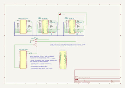
Found out that MR BIOS was available for Gigabyte GA-586HX, so decided to try to figure out a way to dual boot MR and the original Award 4.51PG BIOS.

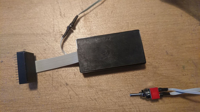
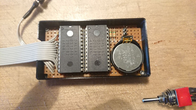
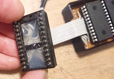
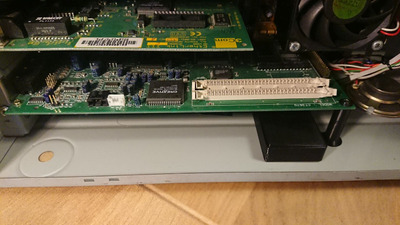
The GA-586HX stores the BIOS on a 1Mbit 29 series EEPROM, SST29EE010. Happened to have a spare SST29EE020, the 2Mbit version of the same chip. Soldered together an adapter to manually switch the highest address pin low/high, effectively splitting the storage area in two parts, and burned a combined MR/original BIOS image to the chip.

MR BIOS works perfectly.

The original BIOS behaves very strangely though, corrupting itself at boot. It'll overwrite addresses 0x0 - 0x7F (128 bytes) and 0x10000 - 0x1007F (128 bytes again) with FF, verified by dumping the corrupted image and comparing it to the original image. It works for one boot after writing the BIOS image to the EEPROM, apparently the corruption happens after shadowing to RAM.

Except for the expected error messages about corrupted configuration - haven't done anything with the settings SRAM yet, it's still shared between the BIOSes - it only complains about "Unknown flash type". It will however complete POST and try to boot the OS.

Got no idea whatsoever what the Award BIOS uses to detect the flash type, but can imagine it's the chip ID bytes. Opened the BIOS image in a hex editor and tried to find any references to the SST29EE010:s chip ID "BF07". Found a couple of instances of that sequence and tried with BIOS images where one, the other, and both instances were changed to the SST29EE020 chip ID "BF10". No luck. Guess those instances were just coincidences, or there's something else that has to be done too.

So, I'm stuck here. Of course I could just completely disable writing by cutting the pin corresponding to /WE from the adapter, but that's not a very elegant solution. Would rather find out what causes the corruption and remedy it. First thing to try is to hack the BIOS to recognize the SST29EE020, alternatively try changing the chip ID of the SST29EE020 to BF07 if possible.

Anyone got any ideas how to go about this? 😀

Reply 1 of 9, by Horun

User metadata
Rank l33t++
Rank
l33t++
kaputnik wrote on 2022-12-20, 21:37:

The original BIOS behaves very strangely though, corrupting itself at boot. It'll overwrite addresses 0x0 - 0x7F (128 bytes) and 0x10000 - 0x1007F (128 bytes again) with FF, verified by dumping the corrupted image and comparing it to the original image. It works for one boot after writing the BIOS image to the EEPROM, apparently the corruption happens after shadowing to RAM.

What are you using to write the Award to eeprom ? A TL866 or some award flasher ? Yes Aflash does check the chip ID and only specific flash apps will work with specific BIOS chips and BIOS iirc.
Could it be your modification is causing the corruption, or maybe some old pc virus you stumbled on ?
Curious why you want to have dual BIOS on a Pentium soc 7 (not even a SS7) that was not designed for it...just wondering

Hate posting a reply and then have to edit it because it made no sense 😁 First computer was an IBM 3270 workstation with CGA monitor. Stuff: https://archive.org/details/@horun

Reply 2 of 9, by kaputnik

User metadata
Rank Oldbie
Rank
Oldbie
Horun wrote on 2022-12-21, 05:18:
What are you using to write the Award to eeprom ? A TL866 or some award flasher ? Yes Aflash does check the chip ID and only spe […]
Show full quote
kaputnik wrote on 2022-12-20, 21:37:

The original BIOS behaves very strangely though, corrupting itself at boot. It'll overwrite addresses 0x0 - 0x7F (128 bytes) and 0x10000 - 0x1007F (128 bytes again) with FF, verified by dumping the corrupted image and comparing it to the original image. It works for one boot after writing the BIOS image to the EEPROM, apparently the corruption happens after shadowing to RAM.

What are you using to write the Award to eeprom ? A TL866 or some award flasher ? Yes Aflash does check the chip ID and only specific flash apps will work with specific BIOS chips and BIOS iirc.
Could it be your modification is causing the corruption, or maybe some old pc virus you stumbled on ?
Curious why you want to have dual BIOS on a Pentium soc 7 (not even a SS7) that was not designed for it...just wondering

Using an Xgecu T56, a successor to the TL866. The "Unknown flash type" message shows during boot after POST though, looks like the Award BIOS itself has some detection routine. Flashing the chip poses no problems at all.

The mod is dead simple. It's just an additional DIP32 socket sitting between EEPROM and mobo, where I cut pin 30 (A17) and wired up a 15k pullup resistor to VCC, and a switch to ground instead. Open switch pulls A17 high through the resistor, closed pulls it low to ground. Measured the voltages on the A17 pin, very close to 5 and 0 volts respectively. There are no unintentional shorts etc. I don't believe this is the problem.

Tried using both a dump from the original BIOS chip and a downloaded image. I'm somewhat limited when it comes to using different versions, need a hacked BIOS to get around the 8.4GB HDD size barrier. Never had any problems with this BIOS on the original 1Mbit chip though, and the corruption happens before the OS loads, so I doubt it's a virus.

Also tried flashing an image with two copies of the Award BIOS. Doesn't matter if it loads from the first or second half of the 2Mbit chip, the corruption happens with the same relative offsets in both cases.

Oh, just want to be able to easily switch back to the original BIOS in case MR BIOS causes compatibility issues with some specific software or something. Also, it's a fun/interesting project, to see if it can be done etc. No matter what, it's at least educational 😀

Edit: Just hit me that those old BIOSes always has this hologram label, with serial number etc. All very serious, probably to assure the customer they got the authentic thing. Gives the impression they might have had problems with counterfeiting. Could it perhaps be some primitive anti counterfeiting measure, bricking the BIOS if it's not loaded from a whitelisted chip, or something like that?

Reply 3 of 9, by quicknick

User metadata
Rank Oldbie
Rank
Oldbie

Just an idea. BIOSes around that time started to store data (ESCD, DMI) inside the flash chip. Maybe the corruption happens because it tries to write something but it fails because of "Unknown flash type".
Also (and I might be very wrong here), couldn't this "dual bios" be implemented by using two SST29EE010 with most of the pins in parallel and playing with the chip enable/output enable pins?

Reply 4 of 9, by Horun

User metadata
Rank l33t++
Rank
l33t++

Yeah in some boards the ESCD/DMI is written to CMOS, others it is written to part of the eeprom (to a gap or at end) though not sure why it is being written to beginning unless it's hitting an addressing issue with the bigger rom size.
If you look at uncompressed Award and AMI bios there are purposeful gaps, some are used for those tables.

Hate posting a reply and then have to edit it because it made no sense 😁 First computer was an IBM 3270 workstation with CGA monitor. Stuff: https://archive.org/details/@horun

Reply 5 of 9, by kaputnik

User metadata
Rank Oldbie
Rank
Oldbie
quicknick wrote on 2022-12-21, 23:47:

Just an idea. BIOSes around that time started to store data (ESCD, DMI) inside the flash chip. Maybe the corruption happens because it tries to write something but it fails because of "Unknown flash type".
Also (and I might be very wrong here), couldn't this "dual bios" be implemented by using two SST29EE010 with most of the pins in parallel and playing with the chip enable/output enable pins?

Horun wrote on 2022-12-22, 00:35:

Yeah in some boards the ESCD/DMI is written to CMOS, others it is written to part of the eeprom (to a gap or at end) though not sure why it is being written to beginning unless it's hitting an addressing issue with the bigger rom size.
If you look at uncompressed Award and AMI bios there are purposeful gaps, some are used for those tables.

That's an interesting idea. It overwrites parts of the actual BIOS program though. The only relevant differences between the 1 and 2 Mbit versions is the additional addressing pin on the latter (which the computer never seens the way I've connected it), and the chip ID. Otherwise they should look identical to the computer. Also, addressing works exactly the same way when writing as reading, and reading the BIOS evidently works just fine, since it boots before the corruption happens. The overwritten parts are obviously critical for the BIOS to boot, so they have to be read correctly.

No, you're not wrong at all, those EEPROMS are designed to be able to run on a common bus. It's really the whole point of the OE pin. It's fully possible to do what you suggest, but I'd have to source those chips, and design an adapter board for them. There are some space constraints too, the GA-586HX BIOS socket sits quite awkwardly in line with the only ISA port the case allows a full length card in. It would probably have to be some ugly external variant connected with a ribbon cable to get it out of the way. Would much rather use a single 2Mbit chip 😀

Reply 6 of 9, by Sphere478

User metadata
Rank l33t++
Rank
l33t++

What about an adapter that has two chips?

I think there are some chips designed to dual boot. Like they have a switching register or something. I recall looking at the datasheet a while back and it seemed to really be made for it. But I can’t recall what it is called now

I think some people might be using this on Amigas? But the chip I found had less pins than the Amiga deal. It looked like a normal bios chip you would use in a 486 or pentium.

Memory is a little fuzzy. Maybe it gives you ideas.

Btw, there is a unfinished rom project in my sig. if you know the solution for the pinout let me know.

Sphere's PCB projects.
-
Sphere’s socket 5/7 cpu collection.
-
SUCCESSFUL K6-2+ to K6-3+ Full Cache Enable Mod
-
Tyan S1564S to S1564D single to dual processor conversion (also s1563 and s1562)

Reply 7 of 9, by kaputnik

User metadata
Rank Oldbie
Rank
Oldbie
Sphere478 wrote on 2022-12-24, 05:27:
What about an adapter that has two chips? […]
Show full quote

What about an adapter that has two chips?

I think there are some chips designed to dual boot. Like they have a switching register or something. I recall looking at the datasheet a while back and it seemed to really be made for it. But I can’t recall what it is called now

I think some people might be using this on Amigas? But the chip I found had less pins than the Amiga deal. It looked like a normal bios chip you would use in a 486 or pentium.

Memory is a little fuzzy. Maybe it gives you ideas.

Btw, there is a unfinished rom project in my sig. if you know the solution for the pinout let me know.

Yep, as mentioned, those EEPROMs can be used on a common data bus. In essence, connect the addressing and data pins of the different chips in parallel on the bus, pull the /OE (Output Enable) pin low on whatever chip you want data from. If a delay of the few milliseconds it takes for the chip to initialize before operation isn't an issue (like in my case), you could control it with the /CE (Chip Enable) pin instead, to keep the chips not in use completely disabled and save a few milliamps. Might be worth considering when you're unsure if the power supply can handle more than one chip at once. With other words, it's technically no problem at all to build an adapter like that, or piggyback the chips leaving the /OE or /CE pins separated. It would however block the only ISA port allowing a full length card unless I do some ugly ribbon cable connected solution, so I'd rather use a single 2Mbit chip instead, and offset the addressing by switching the highest significant address pin manually 😀

The C64 cartridge port is an interface to connect an external 27 (or 28) series parallel (E)EPROM without any peripheral circuitry. They work very similarly to the 29 series EEPROMs used for BIOS storage on old mobos, the only relevant difference is basically the pinout. 128 kbit carts often uses two 64 kbit (E)EPROMs on a common bus as described above.

Which project exactly do you mean? The "How can I flash this motherboard's Bios" one? Looks like you got it figured already. If not, you have the answer above. Basically pulling the /OE pin low makes the chip's output pins leave the high impedance state, effectively connecting them to the bus, and present data on it 😀

I'm at sea the upcoming two weeks, came onboard yesterday. Once I'm back home and finish the project - also need to figure out how to run two Dallas RTC:s in parallel, if their oscillators can run on the same crystal out of specs, etc - I might find time to do a writeup on my dual BIOS project, explaining everything in detail, including some basics on how parallel (E)EPROMS work. Once you wrap your head around the basic concepts, it's not complicated at all.

Reply 8 of 9, by Sphere478

User metadata
Rank l33t++
Rank
l33t++

Re: How can I flash this motherboard's Bios?

Okay 😀 thanks! I’ll cross link the thread.

Sphere's PCB projects.
-
Sphere’s socket 5/7 cpu collection.
-
SUCCESSFUL K6-2+ to K6-3+ Full Cache Enable Mod
-
Tyan S1564S to S1564D single to dual processor conversion (also s1563 and s1562)

Reply 9 of 9, by kaputnik

User metadata
Rank Oldbie
Rank
Oldbie

Finished the hardware part of this. Except for the corruption problem (that I worked around by isolating the Write Enable pin until I got a better solution) it's working perfectly. Now I can swap BIOS by flicking a switch 😀

First there's an adapter made from a DIP32 socket sitting between the for splitting the storage area of the 2Mbit EEPROM in two equal parts for the 1Mbit BIOS images. It's not much to see really.

Then there's an adapter to run dual Dallas DS12885 RTC:s. Those also stores the BIOS settings, so needed two of them. Took a gamble the pins are tristated when the chip isn't enabled. The datasheet didn't suggest anything of the sort, and I can't see any apparent scenarios where you'd want several RTCs on the same bus, but apparently they were. Since I had a few spare suitable xtals, I never experimented with having the RTCs share a single one. A few pics:

DSC_0072.JPG
Filename
DSC_0072.JPG
File size
252.17 KiB
Views
456 views
File license
Fair use/fair dealing exception
DSC_0074.JPG
Filename
DSC_0074.JPG
File size
232.69 KiB
Views
456 views
File license
Fair use/fair dealing exception

Finished and installed in a 3d printed box.

DSC_0076.JPG
Filename
DSC_0076.JPG
File size
203.33 KiB
Views
456 views
File license
Fair use/fair dealing exception

The mobo socket connector.

DSC_0078.JPG
Filename
DSC_0078.JPG
File size
225.92 KiB
Views
456 views
File license
Fair use/fair dealing exception

Installed in the computer. A DPDT on-on switch on the front of the case switches between the BIOSes and RTCs.

Threw together a schematic too. Can't guarantee it's completely correct, since I did it after putting together the hardware. Really got to learn Kicad, figured this was a great newbie project:

schematic.jpg
Filename
schematic.jpg
File size
538.92 KiB
Views
421 views
File license
Fair use/fair dealing exception