Reply 20 of 253, by devius
Rank
Oldbie
- Rank
- Oldbie
I have a controller card with the Goldstar 82C711 chip, which is mentioned as being for motherboards in the datasheet.
I have a controller card with the Goldstar 82C711 chip, which is mentioned as being for motherboards in the datasheet.
mkarcher wrote on 2023-04-19, 19:38:The PT-626, as seen on https://skylots.org/6568006432/PT-626-Hard-Di … ntroller---0557 , uses the UMC UM82C871F VL IDE chip. The UM82C863F listed in the original table is the ISA I/O chip for everything but IDE.
Thanks, I'll fix my list
mkarcher wrote on 2023-04-19, 19:38:A EVLSIO-V3-HJ2, as shown in https://www.flickr.com/photos/181652282@N07/49368874853/ (also take a look at the other photos in that stream). My copy has standard black jumpers instead of the cool blue ones. It has the PDC20630, acompanied by the Goldstar Prime 2 ISA I/O chip.
Looking at that picture, I read the markings on the chip as PDC20230c. Am I misreading it?
And looking at this picture of the VLMIO card: https://www.flickr.com/photos/181652282@N07/4 … in/photostream/
I see jumpers for mode 0-3. Does that mean it only does PIO-0 thru 3 and no PIO-4 ?
p.s. nice pictures. Very rich color.
douglar wrote on 2023-04-19, 20:54:mkarcher wrote on 2023-04-19, 19:38:A EVLSIO-V3-HJ2, as shown in https://www.flickr.com/photos/181652282@N07/49368874853/ (also take a look at the other photos in that stream). My copy has standard black jumpers instead of the cool blue ones. It has the PDC20630, acompanied by the Goldstar Prime 2 ISA I/O chip.
Looking at that picture, I read the markings on the chip as PDC20230c. Am I misreading it?
No, you are correct. The pictures I linked do show a PDC20230C, on the other hand, my card using the same PCB has a PDC20630. Those chips seem to be pin compatible except for the jumper space. My card has a different set of jumpers populated compared to the card on the flickr stream. I found an image that is more like my card here: https://retronn.de/imports/hwgal/hw_controlle … _vlb_front.html
douglar wrote on 2023-04-19, 20:54:And looking at this picture of the VLMIO card: https://www.flickr.com/photos/181652282@N07/4 … in/photostream/
I see jumpers for mode 0-3. Does that mean it only does PIO-0 thru 3 and no PIO-4 ?
p.s. nice pictures. Very rich color.
To be clear: Those are not my pictures. I found them using google.
Yes, that means you can not jumper the card to support PIO-4. You might be able to enable PIO-4 using software drivers, but I consider that unlikely. By the way, it seems the PDC20230C only supports up to PIO 2, and the PDC20630 supports up to PIO 3, if you believe the documentation at https://web.archive.org/web/20100122044951/ht … /pdc20230c.html and https://web.archive.org/web/20100122044951/ht … b/pdc20630.html (PIO 3 being "speed 8" which is only mentioned for the 630 chip).
douglar wrote on 2023-04-19, 17:01:Can you think of any benchmark that will show that 16bit VLB transfers perform the same as 32bit transfers?
*with period correct drive 😀
speedsys
http://rayer.g6.cz/programm/programe.htm rawspeed
Promise EIDE2300Plus would be ideal because https://www.pcorner.com/list/UPLOAD/2300EIDE.EXE/README.TXT/
>device=C:\EIDE2300\EIDE2300.SYS [/F] [/W] [/P] [/D0:n or /M0:m] [/D1:n or /M1:m] [/X2]
"W : EIDE2300PLUS controller works in the 16-bit data access mode.
Certain motherboard CPUs(for example, IBM 486 SLC2) have a 16-bit
external data bus and cannot operate in the default 32-bit data access mode."
I expect little to no difference on <5MB/s drive with ~DX2/66 when adding "/w" parameter. Of course this driver does more optimizations so comparing with/without will show huge difference, but we are only interested in 16-32 bit.
Why do I think that? Because Cirrus Logic Re: Good VLB card benchmark
>MOVSW mem (hit) => Vid: 15.9 MByte/s
>MOVSD mem (hit) => Vid: 15.9 MByte/s
and this is transferring to ram and not slow HDD
douglar wrote on 2023-04-19, 17:01:Ultimately, my goal here is after documenting what VLB controllers are out there, is to:
- Find a fast VLB controller and a slow VLB controller using synthetic benchmarks
I wouldnt expect much difference between controllers as long as all support same timings, quality/optimization of shipped drivers is another story. CPU mode and instructions used can play a huge role
https://www2.math.uni-wuppertal.de/~fpf/Uebun … 2/opcode_i.html
https://fragglet.github.io/dos-help-files/ala … x_at_L837a.html
https://fragglet.github.io/dos-help-files/ala … x_at_L8376.html
worst case scenario is ~30 cycles if you happen to be running anything trapping IO (sb emulation etc, probably windows without 32bit access enabled and working). Thats what, 1.3million instructions on 386DX40? ~2.6MB/s word transfers in V86 mode. Even worse on 486 25MHz 25mhz/30 = ~1.6MB/s words or 3.3MB/s dwords. I guess now I have my answer 😀 32bit transfers are useful on really slow CPUs in worst case scenario.
On the other hand 486 25MHz in pure protected mode should do ~5MB/s with just "rep insw".
DX2-66MHz ~4.5MB/s absolute worst case "rep insw", ~15MB/s best case scenario in protected mode. I hope Im counting this correctly 😜
douglar wrote on 2023-04-19, 17:01:[*]Do a repeatable common real world "makes you wait" task that has a storage dimension (aka cold booting Windows 98 with 16MB RAM)
win98 on 486 pushes definition of real world a little bit 😀 nevertheless I cant wait to read the results.
douglar wrote on 2023-04-19, 17:01:Here are the notable factors that I see for VLB storage benchmarking: […]
Here are the notable factors that I see for VLB storage benchmarking:
- ATA Protocol
- Controller (for VLB controllers)
- Bus Speed
- Driver ( BIOS / BIOS + Shadowing / Drive Overlay / DOS driver / Protected Mode Driver )
- environment. CPU execution mode can have huge impact. Pure Dos, Dos with SBEMU/EMM386/whatever forcing V86 mode, Windows 3/WfW3.11 with/without 32bit access enabled or dedicated driver, Win9x. In case of Win3 and wdctrl take into consideration its very fragile and will not be enabled if it doesnt like something trivial https://www.os2museum.com/wp/how-to-please-wdctrl/
- drive. Slow one, fast period correct 5MB/s, fast 15-20MB/s, fast CF card and maybe even SSD with with sata-to-ide converter.
- write testing? would be very annoying, ideally you would have to restore/wipe drive image before every iteration.
douglar wrote on 2023-04-19, 17:01:I suspect that for any reasonably fast CPU and Storage device, the importance ranking will go Bus Speed + ATA Protocol, and then Driver + VLB controller
my bets are on driver quality dominating
douglar wrote on 2023-04-19, 17:01:If one configuration shows an improvement over another with a 133Mhz CPU, does it still show a similar improvement with a 33Mhz 486 or does it all fade into the background noise with the slower CPU?
And where is the cut off for storage? If the controller matters with a 16GB SSD, does it still mater with a 6GB Quantum Fireball ? With an ST3600A ? With a Caviar 280?
Great idea!
Opti 82C465MV VLB Opti 82C611A VLB https://github.com/torvalds/linux/blob/789b4a … a_legacy.c#L862
This thread is going well. : )
I have few more VLB controllers. Some are not listed here. Feels like time is right for a brief examination ...
To rasz_pl - i also had similar thoughts before.
I can see how reducing calls will make more sense in multi-threaded/tasked environment, but never spent the time to see how this plays in DOS really.
The best way to check this is with Promise 20630 controller + DOS driver.
EIDE2300Plus does not offer ways to switch between 16/32-bit data handling. No jumpers, or DOS driver flags.
The DOS driver for 20630 provides arguments for that.
I doubt any of it made difference back in the day with the slow mechanical HDDs.
Today with fast CF cards we can saturate the controllers and buses, so the difference between the different models is much more prominent.
rasz_pl wrote on 2023-04-19, 21:35:
That's a nice list there. Interestingly some controllers are tagged ATA_PFLAG_PIO32.
Seems to suggest that Linus only used 32 bit IO with the Promise, QDI, and Winbond controllers.
btw - I've been updating the first post -- List of VLB IDE Controllers
Great VLB prices back in 1998!!
https://web.archive.org/web/19971011205936/ht … ountCenter.html
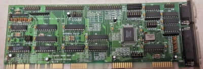
Looking at the Winbond VL400GW/S1336, seems like the card doesn't have a dedicated IC for the IDE controller.
It's also ISA, not VLB
See my graphics card database at www.gpuzoo.com
Constantly being worked on. Feel free to message me with any corrections or details of cards you would like me to research and add.
its VLB all right, PAL is doing all the work, no 32bit transfers here
I saw this chip on a VSI-PV1 VLB board for sale on ebay:
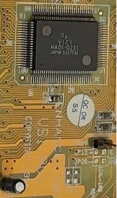
Would the manufacturer be VIC and the part number HAOI-0221 ?
I consider it borderline to call the ST300ALI an "Local bus IDE controller". While the Tekram DC-680T is a caching IDE controller, the ST300ALI is more like a "single-chip 186 system controller". It handles interfacing the cache RAM to the VL bus, the 80186 processor and the IDE ports, provides buffer space for the IDE registers that are used to communicate with the host, contains a 2KB stub ROM, generates IRQs to the 80186 when the IDE command register is accessed or an IDE reset is requested, and forwards IDE device register access from the 80186 to the IDE connectors. It does not forward VL cycles directly to the IDE cables, though. There are variants of the ST300ALI called ST100AII (ISA) and ST200AEI (EISA).
Those chips are likely not designed by ST, but by DataCare (they got acquired by Tekram). It's possible that ST manufactured those ASICs, though.
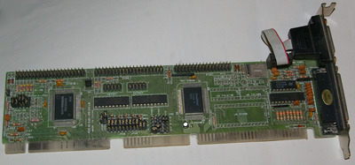
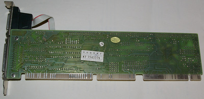
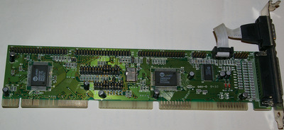
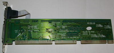
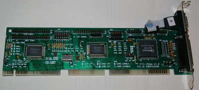
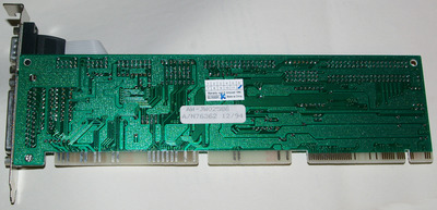
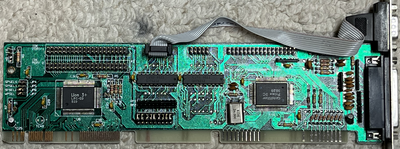
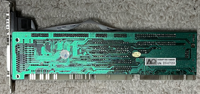
Pictures of my VL-IDE controllers:
Promice PDC20630-based controller:
UMC8672F-based controller:
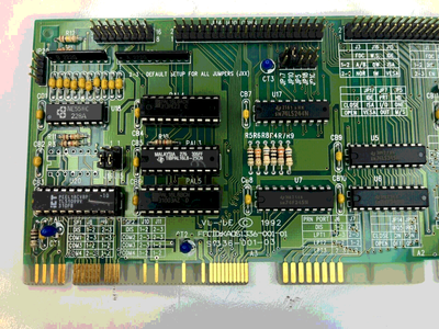
... Winbond W83759F-based controller:
I got this in the mail today:
Someone has a bunch of them on ebay.
I put the drivers here:: http://www.vogonsdrivers.com/getfile.php?file … menustate=56,55
Along with this manual:
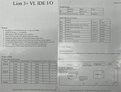
The write protect jumper is kind of unique.
Looks like all of the data lines are connected, so 32bit transfers seems plausible.
Looks like it should do at least PIO3 speeds, but "IDE Mode 3 IDE Hard disk support is a little vague"
It's got 8 speed settings, but I don't understand what it means by "R/W cycle(clock)".
R/W cycle(clock) = wait states.
The smaller this number is, the better.
Also, it looks like the driver and jumpers mirror the same functionality - you can set speed with the jumpers and not use the driver.
But, looking forward to hear more about this guy. Share some details once you test it.
pshipkov wrote on 2023-04-23, 06:31:R/W cycle(clock) = wait states.
The smaller this number is, the better.
If it says "cycle", these numbers probably specify the "cycle" time. That is the time between the start of transferring one 16-bit word to the time of transferring the next 16-bit word. It consists of the "active" time, that is the time when the control signals for read/write are active, and the "recovery" time, that is the duration between the end of one data transfer and the start of the next one. To correctly implement a PIO mode, both the active time and the recovery time need to be no shorter than specified by the ATA committee, so just calculating the cycle time from the numbers given here does not necessarily imply that the controller fully complies with a PIO mode having the same cycle time. "(clocks)" refers to the unit in which the cycle time is given, in this case the duration of the VL clock period. The VL clock period is 30ns for 33MHz FSB, 25ns for 40MHz FSB and 20ns for 50MHz FSB. So the table from the manual for that Lion 3+-based card can also be written as
Speed number cycle time (33MHz) cycle time (40MHz) cycle time (50 MHz)0 1080 900 7201 960 800 6402 810 675 5403 690 575 4604 540 450 3605 420 350 2806 270 225 1807 150 125 100
It is likely that speed 6 at 50MHz resemble PIO3 timings well enough to be working with all PIO3 drivers. Speed 7 exceeds PIO3 already at 33MHz, but might work outside of specification with many PIO3 drives and all PIO4 drives.
John Wehman (dude worked for Seagate since 1988 for ~30 years, currently at Phison) talked about this method of setting speed in 1995 usenet post (comp.sys.ibm.pc.hardware.storage) :
wrote:Here's the tricky part about Promise...they clock the I/O cycles off the Motherboard Bus clock, and blindly say "Fastest transfe […]
Here's the tricky part about Promise...they clock the I/O cycles off the
Motherboard Bus clock, and blindly say "Fastest transfer shall be: three clock
cycles for assertion of IO (R/W) and three clock cycles for de-assertion of same."
On a 33MHz Bus-clock (486-33DX, 486-66DX-2), this computes to 90ns ON, 90ns Off, or
180 ns Cycle time (1/33MHz = 30ns). That's fine, except where 1)the drive can support
PIO Mode 3, but at a reduced t0 cycle time (as reported in ID Data), or 2) the drive
can achieve faster transfer rates (as your drive below).However, on a 50MHz bus, this timing becomes (20ns*3)=60ns ON and 60ns off, or 120ns,
Mode 4 (sort of). With a faster drive (as below), this would be okay, but put just
about any other drive on, and your talking C.O.R.R.U.P.T.I.O.N.
Really curious what pre-fetch and post write are all about, maybe its implemented in the driver because I have little hope of that chip containing whole sectors worth of cache.
rasz_pl wrote on 2023-04-23, 12:51:Really curious what pre-fetch and post write are all about, maybe its implemented in the driver because I have little hope of that chip containing whole sectors worth of cache.
Pre-fetch and posted writes are a hardware feature. The only thing the driver does about them is turn them on (so that the chip can deliver sensible performance), or turn them off (to avoid chip bugs or interface with really strange old drives). Your post Re: List of VLB IDE Controllers shows that you obviously are not that deep into how VL IDE interface chips actually operate internally, and why stuff like 32-bit access does make a lot of sense. So I will start at the basics: You mention "a transaction every 30ns", which likely implies you are thinking about 33MHz VL clock, which makes a lot of sense. 33MHz is a very common VL bus frequency that allows stable operation in most sensible circumstances. Let's also assume a processor without clock doubling, as the 486DX-33 was very common those days.
A VL transaction takes at least two cycles. VL is a synchronous bus: Signals levels only matter at the point of the rising edge of the clock signal. The signals must be valid some nanoseconds before the rising edge of the clock signal (called "setup time") and must be valid one or two nanoseconds after the rising edge of the clock signal (called "hold time"). The fastest type of VL access is one rising clock edge at which the device (e.g. the IDE controller) gets told that it should perform some action (at this edge, the /ADS line is low to indicate the start of a cycle), and in the next cycle the device acknowledges that the action has been successfully perfomed (at this edge, the /LRDY is low to indicate the end of the cycle). There is no pipelining on the VL bus: The address lines and cycle type indication lines like M/IO or R/W are valid until the rising clock edge in which /LRDY is low. So the fastest cycle on the VL bus is 60ns, and the duration between the time at which the IDE interface chip can assert /IOR to the drive and the time the data must have arrived from the drive would be one clock period, i.e. 30ns. This would also be the "active time". The IDE specifcation requires an active time of 70ns in PIO mode 4 and even 80ns in PIO mode 3. This is 40 or 50 ns more than the active time in a 2-clock VL cycle, so we need to add 2 extra wait states to VL cycle if the VL IDE interface works as a dumb bus extender. ISA IDE interface cards usually do work as dumb bus extenders, because that's the original idea of IDE. At this point, it's obvious that a dumb VL/IDE adapter can't perform a transaction every 30ns, as you assumed, but that the IDE transaction itself already takes 120ns.
You are typically reading data using REP INSW from an IDE port (I use reading as example, because usually reading dominates, and because the bottlenecks are thighter on reading). This means the CPU does not only perform the IDE transaction on its front-side bus (which takes 120ns), but it also needs to write the data it obtained from the IDE drive into RAM. As I am assuming a standard 486DX-33, the L1 cache is operated in write-through mode. There is no write merging in the 486 processor, so every 16-bit value obtained from the IDE drive is written to RAM using a 16-bit write transaction. As the VL bus is basically the same as the 486 FSB, it is still valid that the minimum transaction time for writing that 16-bit word to memory is 60ns. This means at 100% FSB saturation, REP INSW operates at a cycle time of 180ns, so this would just barely hit PIO3 timings. Well, in theory. In practice, I sneakily postulated a non-clock-doubled DX-33. Looking at the Intel-provided instruction timings, REP INSW operates at 8 clocks per iteration if everything goes to plan. This means the fastest the 486DX-33 can do on REP INSW is 240ns per cycle, the cycle time of PIO mode 2. This only applies if (as I just wrote), if everything goes to plan. It doesn't, though. The IDE read adds two wait states, which likely directly hit the INSW throughput, so basically that fastest a 486DX-33 processor can obtain on a PIO3-capable drive if the VL IDE interface performs the IDE transaction during the VL transaction is a cycle time of 300ns, which is worse than PIO2. Now, could you also get a cycle time of 300ns from a PIO2 drive? Sorry, no. The theoretical maximum active time at 2WS is 3 clocks or 90ns. A PIO2 drive can rely on the active time being at least 100ns, so another wait state is required. The net result is: Using a dumb VL controller, you get 300ns cycle time for a PIO3 drive, and 330ns cycle time for a PIO2 drive. This is less than spectacular.
There are two obvious observations to make:
And that's where the features of all good VL IDE chips get relevant:
So a read-ahead buffer of 32 bits is enough: It takes two IDE words of data, waiting for the 486 to perform the next REP INSD iteration, which can then be answered without any wait states. The buffer is then refilled as soon as possible. The same is true for the post-write buffer and REP OUTSD. REP OUTSD can be performed faster (at 5 clocks per cycle, that is 150ns cycle time), if the data to output is currently cached in L1, though.