Reply 40 of 57, by mkarcher
pc2005 wrote on 2023-10-03, 17:32:A recheck for CPU control signals and specially for cache would be appreciated (my board ATC-1415 has only one cache bank so I could not find control signals for the second one, also it
has only 2 SIMM slots). Some CPU signals are routed through jumpers, so I could miss few.
Thanks for writing up that stuff. I have some notes on that chip, too, which could help you:
51 = /COE (second bank)58 = /CCE (second bank)59 = CA0 (first bank or only bank)61 = CA0 (second bank) or CA1 (single bank)
The way I number the cache address lines, there is no CA1 in dual-bank operation. There are no further /RAS and /CAS pins for four slots. My notes on the Biostar MB-8433-UUD indicate that there are four RAS signals and eight CAS signals.
For memory organization on the 8881, you should be aware that there basically are just two "chipset banks", but each chipset bank (which has a fixed size per rank) can contain up to four(!) memory ranks. In a 4-slot board, there are two pairs of memory slots that need to be equipped with modules with identical bank layout (if both sockets are equipped at all). The chipset can map the chipset banks to
- The first rank of the first slot of a bank
- The first rank of the second slot of a bank
- Both ranks of the first slot of a bank
- Both ranks of the second slot of a bank
- The first rank of both slots of a bank
- Both ranks of both slots of a bank
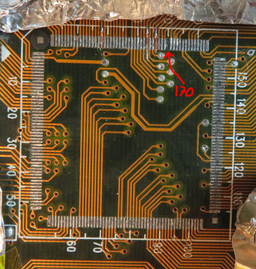
According to my notes, there is one set of RAS signals (two pins) per chipset bank, one set of CAS signals for the "first slot" of each bank and a second set of CAS signals for the "second slot" of each bank. It seems that your board only populates the first slot of the first bank and the second slot of the second bank, which allows maximum flexibility, as there are no paired slots, and optimal distribution of the load on the /CAS signals. My notes do not indicate anything about /WE for the RAM, but having a second /WE for four-slot systems on pin 170 might be possible, albeit unlikely given that your board already equips both chipset banks and all /CAS signals.
The note about pin 198 (R/W#) having a jumper is likely for CPUs with L1WB. It is usual to connect INVD with R/W#.
pc2005 wrote on 2023-10-03, 17:32:If you use 486-/PODP-Pinout and Differences as 486 pinout source, careful I think A16 and A13 are swapped there.
Indeed, they are. I already fell into that trap.
Here are my notes on chipset programming registers (no warranty on completeness and/or correctness), includes both the 8881 and the 8886:
North Bridge============50.80 L2 cache enable50.40 L2 cache mode (WT/WB)50.30 Cache read burst (3-2-2-2/3-1-1-1/2-2-2-2/2-1-1-1)50.08 Two banks of cache50.07 L2 cache size (none/64K/128K/256K/512K/1024K/resvd/resvd)51.C0 Read WS (3/2/1/0)51.30 Write WS (3/2/1/0)51.04 A0000-BFFFF(?) PCI write merge51.02 Set after memory test, cleared for L1WB51.01 Tag allocation (7Tag+1Dirty/8Tag+0Dirty)52.80 CPU to PCI Post Write (1WS/0WS)52.70 bank 2/3 total size (1M/2M/4M/8M/16M/32M/64M/128M)52.08 swap banks 0/1 with 2/352.07 bank 0/1 total size (1M/2M/4M/8M/16M/32M/64M/128M)53.80 CPU to PCI Burst Write53.40 Burst copy back option53.20 swap bank 2/353.10 swap bank 0/153.0C bank 2/3 row mode (1*double sided/1*single sided/2*single sided/2*double sided)53.03 bank 0/1 row mode (1*double sided/1*single sided/2*single sided/2*double sided)54.80 DC00 shadow read enable54.40 D800 shadow read enable54.20 D400 shadow read enable54.10 D000 shadow read enable54.08 CC00 shadow read enable54.04 C800 shadow read enable54.02 C0/C4 shadow read enable54.01 ESEG shadow read enable55.80 FSEG shadow read enable55.40 Global shadow write protect55.20 System BIOS cachable55.01 Video BIOS cachable56.FF Memory hole base (in 64K blocks)57.80 Memory hole enabled/disabled57.70 Memory hole size (64k/128k/256k/1M/2M/4M/8M/off)58.FF 0F if system BIOS cachable59.FF 00 if system BIOS cachable5A.40 Force cache hit5A.10 Enable memory parity5A.02 Some kind of deturbo5A.01 Cleared during processor clock measurement5C.FF SMRAM base A27..A205D.80 Early Cache Write mode5D.10 Slow Referesh5D.0F SMRAM base A31..A2860.20 Set when enabling classic AMD SMRAM60.02 Disable memory(?) parity
60.01 Open SMRAM space61.C0 EDO mode? (no/resvd/resvd/yes)61.08 EDO speed (4-2-2-2/3-1-1-1)61.02 Cyrix L1WB mode62.01 Set on early boot for revision "E"62.02 Burst mode (interleaved/linear)South Bridge============40.10 Set on B2 revision, but cleared if no PS/2 mouse40.04 PCI posted memory write40.03 IBC devsel decoding (medium/slow/fast/resvd?)41.40 Disable parity check (maybe PCI SERR#?)41.04 Enhance PCI performance (enabled/disabled) // PCI bus park option (enabled/disabled)43.F0 INTA target IRQ43.0F INTB target IRQ44.F0 INTC target IRQ44.0F INTD target IRQ45.04 Set on B2 revision45.01 Set on B2 revision, but cleared if no PS/2 mouse46.80 PM IRQ (10/15)46.40 PM interrupt method (SMI/IRQ)46.10 Preempt PCI master option46.08 INTD enabled46.04 INTC enabled46.02 INTB enabled46.01 INTA enabled47.40 Enable flash writes (0=enabled, 1=disabled). Interop with 57.4 unknown.47.08 INTD level triggered47.04 INTC level triggered47.02 INTB level triggered47.01 INTA level triggered50.80 Set if PCI video BIOS is installed50.01 Set by bootblock after51.FE Size of RAM in units of 4M (rounded down, exception: 4M if rounding down results in 0M)56.8056.60 Cleared by boot block, under some circumstances set by video card setup56.0C KBD clock (7MHz/by4/by3/by2)56.03 ISA clock (by3/by4/by2/resvd?)57.20 Set to flash. For whatever reason57.10 Set on B2 revision57.08 Keyboard Emulation57.04 Some bit used for flash write protection (Guessed: GPO, but seems wrong)8886AF/8886BF: Shuttle HOT433 and Biostar UUD8433: Set = Protected, Clear = Writeable8886F: Gigabyte GA486IM: Clear = Protected, Set = Writeable57.03 IO recovery time (2BLCK/4BCLK/8BCLK/12BCLK)70.80 Monitor PCI4 master activity70.40 Monitor PCI3 master activity70.20 Monitor PCI2 master activity70.0F Green Timer minutes (0.5/1/2/4/8/16/32/64/128/256/512/rsvd/rsvd/rsvd/disable/0.25)71.80 Monitor PCI1 master activity71.40 Monitor LPT access71.20 Monitor COM access71.10 Monitor ISA DMA master access71.08 Monitor IDE access71.04 Monitor Floppy access71.02 Monitor Graphics card access72.80 Monitor extra region A972.7E Monitor extra region mask (1=don't care for A0..A5) Really A0?72.01 Monitor VL slave access73.FF Monitor extra region A8-A174.01 Monitor ISA shared memory access (A0000-D0000)76.40 Set in flash-related code76.30 SMI interface mode (Intel/Cyrix classic/?/AMD classic)76.08 Will be set by non-PCI VGA access? Cleared and probed in write-merge setup code76.04 Cleared by APM init76.02 Set by APM CPU idle, cleared by APM init82.03 Set on B2 revision to 390.08 Wake-Up on IRQ390.10 Wake-Up on IRQ490.20 Wake-Up on IRQ590.40 Wake-Up on IRQ690.80 Wake-Up on IRQ791.01 Wake-Up on IRQ891.02 Wake-Up on IRQ991.04 Wake-Up on IRQ1091.08 Wake-Up on IRQ1191.10 Wake-Up on IRQ1291.40 Wake-Up on IRQ1491.80 Wake-Up on IRQ15A0 Set to 0 by Boot BlockSet to 34 by APM init (SMI mask?, 1 = enable)A2.01 SMM event 0A2.02 SMM event 1A2.04 SMM event 2A2.08 SMM event 3A2.10 SMM event 4A2.20 SMM event 5A2.40 SMM event 6A2.80 SMM event 7A4.03 CPU-to-PCI (2:1/1:1/3:2/resvd?)IDE controller (only on 8886BF)===============================41.80 Enable primary channel41.40 Enable secondary channel41.04 Cleared above PCI3342.FF Set to 33 on boot43.C0 Something for PM (0=fast, 3=slow)43.30 Something for PS43.0C Something for SM43.03 Something for SS44.F0 Another thing for PM (2=fast, 12=slow)44.0F Another thing for PS45.F0 Another thing for SM45.0F Another thing for SS46.F0 Third thing for PM (0=fast, 12=slow)46.0F Third thing for PS47.F0 Third thing for SM47.0F Third thing for SS48-49 just like 44-454A-4B just like 46-47IO 108, key: 4A/6C (only before 8886BF)==================B0.40 Enable secondary IDE channelB2.F0 Something for PM (0=fast, 4=slow)B2.0F Something for PSB3.F0 Something for SMB3.0F Something for SSB4.F0 Another thing for PM (3=fast, 12=slow)B5.0F Another thing for PSB6.F0 Another thing for SMB6.0F Another thing for SSB7.F0 Third thing for PM (2=fast, 12=slow)B7.0F Third thing for PSB8.F0 Third thing for SMB8.0F Third thing for SS