First post, by mpe
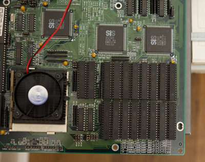
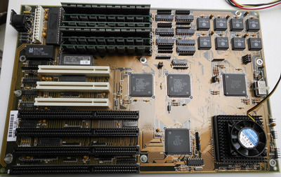
I've just got this cool motherboard (Elitegroup SI5PI AIO) and I am on a mission to upgrade the L2 cache to 2048k. The maximum documented suze for this board is 1M (either in single or dual-bank config), but the DIP32 sockets are there and there are reports that this might be possible so I am trying.
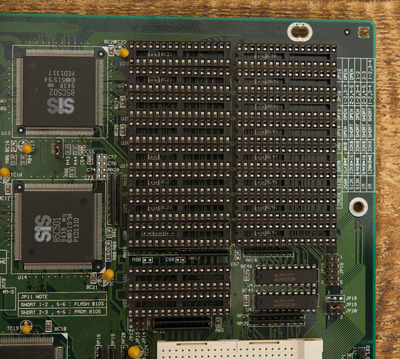
Getting 16 or 18 128K x 8 chips wasn't easy as the (fakes?) IS61C1024 from eBay have like 30-40% defect rate. But I ordered enough spares to have 18 working chips which work fine in 1024k mode and on other boards.
Now I am trying to figure out the jumpers. There are two sets of jumpers. One of them JP13, JP14 (and unsoldered JP12) seems to be configuring the tag SRAM size. They are wired directly to D58, D61 and D62 pins of the CPU.
The second group of jumpers (JP15 and JP16) seems to be wiring together high address bits of data SRAMs. Using multimeter I made this drawing.
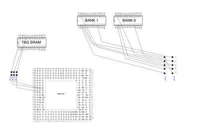
My best guess is that the setting for 2MB is JP15 - 2-3, 4-5 and JP16 2-3, 4-5. JP4 SHORT, JP13 SHORT and I am not quite sure about JP12. Depends if I need 16th address bit of TAG.
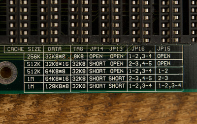
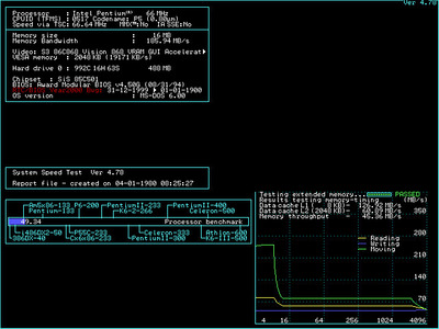
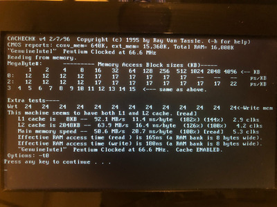
When I put all chips in, the BIOS indeed reports 2048k, but hangs during booting to DOS (or later when skipping config.sys). So something isn't quite right.I tried to open/shorten JP12, enable/disable write-through, insert/remove dirty cache SRAM. But nothing helped.
Now my questions.
1. How big (address size) tag and dirty cache chip a Pentium system with 2M cache needs? Is 2 x 32kx8 enough?
2. Any idea if my jumper setup is correct?
3. How do actually motherboards detect cache size? Looks like they must be sampling address bits of cache chips at some point during boot. Would love to understand how this works.