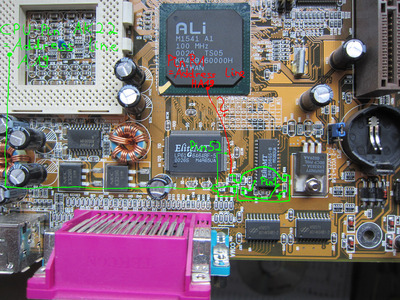
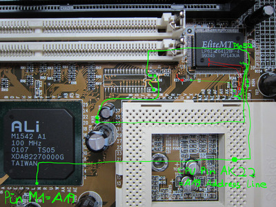
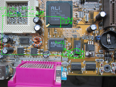
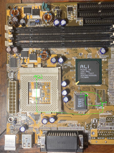
Finally after more than one year, I had some time during last week to do some measurements on my Jetway 542C and Gigabyte GA-5AX in order to find the A19 address line and its connection points to L2 cache, TagRAM, and northbridge: On the green lines I measured an electrical resistance of 0 Ohm (okay it was 0.2 Ohm 😉 )
As you can see, there are some differences starting at the CPU:
- L2 cache chip on the Gigabyte is separated by an extra resistor R46 from A19 line whereas on the Jetway R304 is in front of both L2 cache and TagRAM chip
- Coming from the CPU, R59 is placed in front of TagRAM Pin 1 on the Gigabyte but R21 comes afterwards on the Jetway
- Passing TagRAM Pin 1 on GA-5AX we come to missing resistor R259. Then address line A19 divides to the 10 kOhm resistor R258 (that has no equivalent on the Jetway) and to a line leading below L2 cache chip.
On both boards, I have no idea which line ends up at northbridge Pin R1 finally.
...and shorted R304. <- This is definitively wrong!!! It should be at least a 11.3 Ohm resistor as I think to know now (EIA-96 code)!🙄 Now I'm completely lost: I measured two other address lines A15 and A14. Beginning at CPU socket via L2 cache to TagRAM I measured an electrical resistance of 0.3-0.6 Ohm increasing with the length of the wire. These are the same values as I get for A19 when shorted with small pieces of wire.
Before I continue adding the external TagRAM, I would like to know some things:
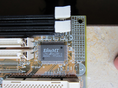
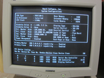
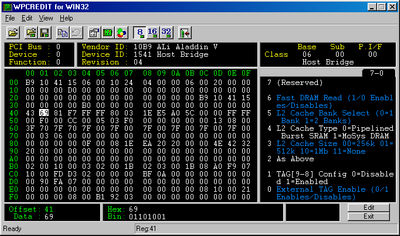
1. As you can see above from WPCRedit screenshot, L2 cache chip was configured as 2-bank pipelined burst SRAM. However, I know that my DFI K6XV3+/66 configures identical chips as 1-bank pipelined burst SRAMs.
According to Aladdin V data sheet,
a pull down resistor with 20k - 60k Ohm must be placed at HA19 address line when using 1-bank pipelined burst SRAM.
This can also be configured in software and I did it already with a BIOS patch but correct hardware detection would be nicer 😀 .
Where should I place it? At R259 on the Gigabyte and R313 on the Jetway?
2. How many Ohm must resistors have that are to be placed at
- Gigabyte R46, R59, and R259
- Jetway R304, R21, and R313?
3. Do I have to remove R258 on the Gigabyte when connecting A19 address line?
4. Has anyone got a defective GA-5AX or 542C without northbridge (or with and can remove it) where one can follow address line A19 to its end point under the northbridge chip?
5. Would anyone owning a 1 MiB Asus P5A measure the A19 address line as I did it in my first post and draw a picture with values of the resistors?
And lots of more questions but this should be enough for now... 😉
Last edited by Lotosdrache on 2021-12-15, 09:39. Edited 2 times in total.
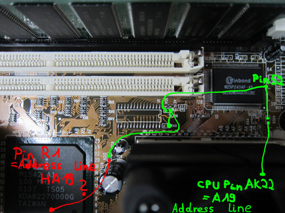
I had a look in M1541 datasheet and HA19 is pin R1. And pin R1 sits on the edge of the chip so you will not have a too hard time to find it 😀
A19 is also on the edge. Sharp thin probe could work?
A19 is also on the edge. Sharp thin probe could work?
By this stage, I didn't thought about connecting TagRAM at all. I hope all lines are already connected. Thanks for finding Pin A19 (= TagWej signal line) on the northbridge. I will try to follow it.
Here comes an update of the electrical diagrams:
I overlooked that Jetway 542C uses M1542 baby AT version of Aladdin V having a different pinout compared to M1541 ATX version of GA-5AX.
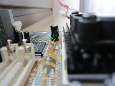
Address line A19 starts at M1542 Pin M1 -> CPU Pin AK22 -> L2 cache Pin 52 -> TagRAM Pin 1 -> back to L2 Cache Pin 41
Here are some branches that I don't understand yet (wires below L2 cache can be seen in first post above where I removed the old cache).
Address line A19 starts at M1541 Pin R1 -> CPU Pin AK22 -> L2 cache Pin 52 -> TagRAM Pin 1 -> back to L2 Cache Pin 40
This is a little bit different compared to 542C. I don't know why there is a possibility of connecting address line A19 to L2 cache pin 40. According to @Roman555's diagrams here and here, Pin 40 should be grounded.
Pin 41 should be connected to VCC3 via 10 kOhm resistor. This may already be the case on GA-5AX. Resistor R47 is labelled with "103".
I have no idea yet how to connect L2 cache Pin 41 to V CC3 on Jetway 542C or why it can be connected to address line A19.
Nice!
@Skalabala Did you solve the stability issues?
Do you also have a 512 kiB one? If so, would you please compare the whole 😉 resistor network in order to find any other differences? 💌
I guess you're going to stay awake this night and hence you will have much time... 😉
Last edited by Lotosdrache on 2022-01-01, 08:36. Edited 1 time in total.
Do you also have a 512 kiB one? If so, would you please compare the whole 😉 resistor network in order to find any other differences? 💌
I guess you stay awake this night and hence you will have much time... 😉
Stability issues huh? My 1.06 is totally worthless. Random crashes all over the place. The 1.04 isn’t perfect but much much better.
Btw lotosdrash, I’m pretty sure that pin connects to more than just pin 40 and 52 on that side. If you want I can map out all the places it goes if that matters
That's funny how different people are! I always tried to find and am still searching for motherboards without onboard sound solutions. In deed, I prefer boards having as less additional chips as possible. Just the chipset nothing else but many free expansion slots to plug in my dream cards.
Exciting progress!!!
I’m pretty sure that pin connects to more than just pin 40 and 52 on that side. If you want I can map out all the places it goes if that matters
That would be interesting. I'm still searching for those connections that set L2 cache and TagRAM configuration in the northbridge registers.
Nice!
@Skalabala Did you solve the stability issues?
Do you also have a 512 kiB one? If so, would you please compare the whole 😉 resistor network in order to find any other differences? 💌
I guess you're going to stay awake this night and hence you will have much time... 😉
If I had a 512kb I would have written a how to 512kb-->1024kb by now :p
The stability is better as I installed a heat sync on clockgen.
I have to test stability with non overclocked CPU and a Geforce mx, the overclocked GF3Ti puts strain on the AGP :p
Lotosdrachewrote on 2022-01-01, 09:01:That's funny how different people are! I always tried to find and am still searching for motherboards without onboard sound solu […] Show full quote
That's funny how different people are! I always tried to find and am still searching for motherboards without onboard sound solutions. In deed, I prefer boards having as less additional chips as possible. Just the chipset nothing else but many free expansion slots to plug in my dream cards.
Exciting progress!!!
I’m pretty sure that pin connects to more than just pin 40 and 52 on that side. If you want I can map out all the places it goes if that matters
That would be interesting. I'm still searching for those connections that set L2 cache and TagRAM configuration in the northbridge registers.
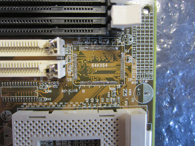
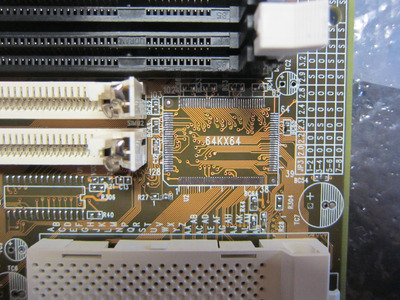
I identified the board that belongs to Roman555's electrical diagrams here and here.
It's Gigabyte's GA-5AA. At least, numbers of all resistors are matching.
Would be nice to get better quality images of all boards especially from the area around northbridge, TagRAM, and L2 cache. It would be perfect if I can read values written on resistors R169, R170, R171, R159, R158 (most likely not populated), and R155. 😀