Reply 60 of 86, by biessea

- Rank
- Member
mkarcher wrote on 2022-09-12, 14:47:Good news: These values are the ones that I need to get to a conclusion. Bad news: These values all look fine, so it doesn't loo […]
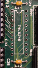
biessea wrote on 2022-09-12, 12:38:If I have understood good I re-tried to measure the diode test and write down all the results:
[...]
I hope it gives you more interesting indication.
Good news: These values are the ones that I need to get to a conclusion. Bad news: These values all look fine, so it doesn't look like your issue is caused with the low address bits of the RAM.
I'm sorry, but at the moment I am out of ideas what to try with the equipment and skill you currently have. The board is very close to working fine, but somewhere is a minor fault, and it is difficult to locate that fault. The next thing I would do if it were my own board: Use an ISA POST card to trace the progress of the self test, and disassemble the BIOS (after reading it in an EPROM reader) to find out what specifically the BIOS is doing before it goes beeping. That means: In this scenario of remote debugging, I have to give up.
Your 386DX-40, the coprocessor and the RAM are still good components, and assuming the fault is on the board (which is quite likely), I would keep looking at ebay, craigslist or similar for another 40MHz-capable 386 board for an acceptable price.
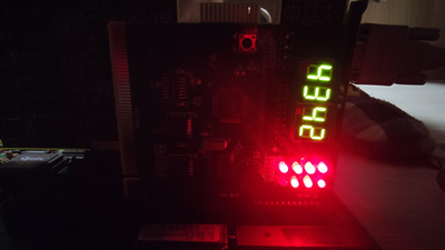
Hey but, if I buy a IDE-ISA post card can you have more ideas then?
It will worth what do you think?
I have a USB bios programmer, ch341a, I use to program video card bioses. Can this help to you my dear friend?
Computer lover since 1992.
Love retro-computing, retro-gaming, high-end systems and all about computer-tech.
Love beer, too.