VOGONS


First post, by feipoa

User metadata
Rank l33t++
Rank
l33t++

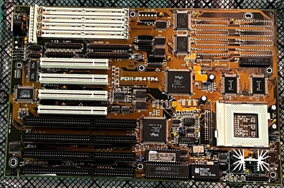
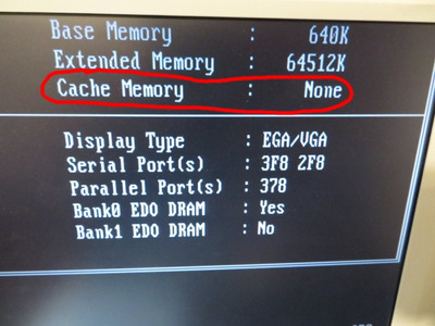
I have an Asus PCI/I-P54TP4 motherboard in a case with an AMD K5-PR200. It is a socket 5 system that I previously modified to have both BF0 and BF1 jumpers, letting the K5 run at 2x. I am planning on another mod for the system. It currently has 512 KB of direct-mapped L2 cache, but there exist QFP pads for pipeline burst SRAM (PB SRAM). I read in the manual that this board can do 256K pipeline burst SRAM, meaning two QFP-100 chips of 32kx32.

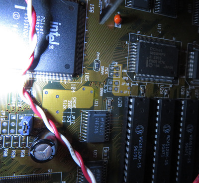
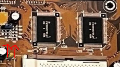
However, there are unpopulated jumpers JP13, JP14, and JP15 as well as unpopulated resistors R57, R58, R59, and R60. With my direct-mapped configuration, only JP12 has a header soldered, as does R61. I am hoping someone has an Asus PCI/I-P54TP4 with factory PB SRAM and could send me a photo of this region so I can see what is populated. The manual only mentions to set JP12 to 256K for pipeline burst SRAM, and has no mention of these other jumpers. However, JP12 is also used to select between 256K and 512K direct-mapped SRAM, thus I am concerned some of these other jumpers or resistors may be needed.

Also, I read on anand tech that the 430FX chips, which is what is used on the Asus PCI/I-P54TP4, can tolerate 512K PB SRAM. If this is true, do you think it would work if I soldered on 64kx32 PB SRAM chips instead of 32kx32?

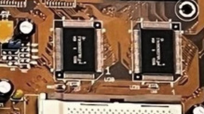
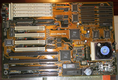
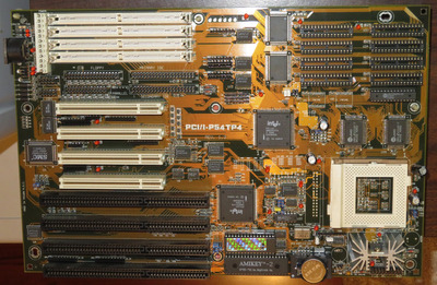
Here's an image of the unpopulated region I am referring to:

Asus_PCI-I-P54TP4_unpopulated_SRAM_jumpers.JPG
Filename
Asus_PCI-I-P54TP4_unpopulated_SRAM_jumpers.JPG
File size
910.73 KiB
Views
1784 views
File license
CC-BY-4.0

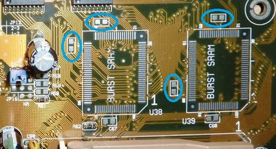
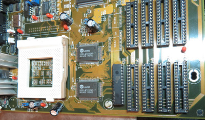
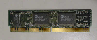
These are the 32kx32 PB SRAM chips I was intending to desolder:

32Kx32_pipeline_burst_SRAM_for_Asus.JPG
Filename
32Kx32_pipeline_burst_SRAM_for_Asus.JPG
File size
145.21 KiB
Views
1784 views
File license
CC-BY-4.0

Plan your life wisely, you'll be dead before you know it.

Reply 1 of 125, by rasz_pl

User metadata
Rank l33t
Rank
l33t

http://www.bitsavers.org/components/intel/pci … HEET_199612.pdf

>CACHE CONTROL REGISTER
>Address Offset: 52h
>Access: SSSS0010 (S = Strapping option)

Strapping means jumpers:

> After a hard reset, CC[7:4] reflect the inverted signal levels on the host address lines A[31 :28].

so just a matter of finding which address lines missing jumpers go

>Bits[7:6] Secondary Cache Size
>0 1 256 Kbytes
>1 0 512 Kbytes

>JP12 is also used to select between 256K and 512K

so JP12 pulls down A[31:30], part of mystery solved

>The default values can be overwritten with subsequent writes to the CC Register

or ignore jumpers completely and enable full cache with debug.exe? it might work in dos if there is some internal logic auto flushing cache on change

> For the 256-Kbyte configurations, an 8kx8 standard SRAM is used to store the tags. For the 512-Kbyte configurations, a 16kx8 standard SRAM is used to store the tags and the valid bits.

dont forget to upgrade the tag 😀

feipoa wrote on 2022-11-11, 04:40:

I am hoping someone has an Asus PCI/I-P54TP4 with factory PB SRAM and could send me a photo of this region so I can see what is populated.

was there one? or is the closest thing this https://theretroweb.com/motherboards/s/asus-p … xe-ver.-2.4-2.5

Last edited by rasz_pl on 2022-11-11, 12:19. Edited 1 time in total.

Open Source AT&T Globalyst/NCR/FIC 486-GAC-2 proprietary Cache Module reproduction

Reply 2 of 125, by majestyk

User metadata
Rank Oldbie
Rank
Oldbie

I recently thought about modifying my PCI-I-P54TP4 and the best pic I could find was this one:

PCI_I_P54TP4_pptotal.JPG
Filename
PCI_I_P54TP4_pptotal.JPG
File size
223.19 KiB
Views
1742 views
File license
Fair use/fair dealing exception

Seems like most of the jumpers are unpopulated here as well. The two buffers/transceiversa are absent on this version.

Reply 3 of 125, by feipoa

User metadata
Rank l33t++
Rank
l33t++

Bummer about the *245 buffers. Would I need to de-solder them if installing PB SRAM?

Good news about the jumper block being unpopulated.

There's another set of jumpers, which I may need to alter. See photo.

Asus_JP8_thru_JP11.JPG
Filename
Asus_JP8_thru_JP11.JPG
File size
504.24 KiB
Views
1714 views
File license
CC-BY-4.0

It looks to be setting the voltage for the SRAM. My board has JP8 and JP9 soldered closed. The board calls this "MIX SRAM". Then there's JP10 and JP11 which are left open and the board calls this 3.3V SRAM. It is not clear to me if "MIX SRAM" is only for mixed-mode SRAM (supply voltage is 5V, but output level is 3.3 V), or if it is also for 5 V SRAM modules, or both options (hence the 'mix'). What do you guys think? I'm using traditional 5 V SRAM in my board now. Was I supposed to use mixed-mode? I'm pretty sure the RAM in this board, when I bought it, was standard 5V.

In either case, the pipeline burst SRAM modules use 3.3 V, so would I need to adjust this as well? I am unable to determine from that photo provided by majestyk which jumper bar is soldered in which jumper locations.

Regarding which size TAG to use, the Asus manual states that I can use either 8k8, 16k8, or 32k8. As such, I would continue to use the 32Kx8 that I currently have installed.

It wasn't clear to me from that 430FX datasheet if two pieces of 64kx32 is supported for 512KB PB SRAM, or if I had to use four pieces of 32kx32. I suspect the latter. Nonetheless, I a 64kx32 chip would use pin 49, which is Address A15, while on a 32kx32 chip, pin 49 is N/C. So I looked at the traces on the Asus board for Pin49, but it appears not to be connected. Thus I am limited to 256K PB SRAM on this board.

Plan your life wisely, you'll be dead before you know it.

Reply 4 of 125, by majestyk

User metadata
Rank Oldbie
Rank
Oldbie

If the PB-SRAMs are directly connected to the VRM output, I wouldn´t bother too much about the voltage jumpers. I assume they are for the DIL chips only. Just make sure the TAG RAM is connected to 5V. It´s the same setup most COAST modules have.

Last edited by majestyk on 2022-11-12, 08:11. Edited 1 time in total.

Reply 5 of 125, by feipoa

User metadata
Rank l33t++
Rank
l33t++

The VRM is set for my AMD K5, so it is at 3.5 V. The other options are 3.4 V and 3.6 V. No 3.3 V as you mentioned.

Did your motherboard come with mixed mode 5V/3.3V DIP SRAM, or 5V DIP SRAM? The use of "mix sram" still has me questioning the use of 5V SRAM.

What is stopping you from upgrading your motherboard? Which PB SRAM modules will you be using?

I remember reading in another thread, ASUS PCI/I-P54TP4 Socket 5 motherboard thread/review , that having the cache enabled slowed the performance down. I was going to test for this next, take some benchmarks, then upgrade to pipeline burst, and compare.

Last edited by feipoa on 2022-11-12, 07:29. Edited 1 time in total.

Plan your life wisely, you'll be dead before you know it.

Reply 6 of 125, by majestyk

User metadata
Rank Oldbie
Rank
Oldbie

There´s a 3.3V PSU connector on both versions but it´s not populated and not used. It was probably meant to power the PCI slots.

Here´s my experience repairing this mainboard:
Re: Asus PCI/I-P54TP4 annoying cache detection error

Modding the board for the second (Vcore) VRM is the true performance booster here.
When the second VRM is in place you can set the onboard VRM to 3.4V for I/O and Vdd power. If you don´t have the second VRM any 3.3V SRAMS or PB-SRAMS will be supplied with the selected core voltage of 3.4 or 3.5V. This is "by design" and should not cause any problems. It means "overvolting" the SRAMS by 6%. Even 32Kx32 PB-SRAMS like the Winbond W25P010 have quite a wide range of operating voltage:

winbond3232.JPG
Filename
winbond3232.JPG
File size
39.1 KiB
Views
1644 views
File license
Public domain

No meed to worry about 3.5V!

The 7nS QFP SRAM chips on your COAST module should be perfect for the job.

I skipped the conversion to PB-SRAM because I had a lot of work finally getting the DIL SRAM to work and because I couldn´t find any good pictures of the PB-SRAM version.

Btw. - revision 1.32 has 4 additional components around the QFP landings (probably capacitors) that are not labeled on my DIL version while they are non exixtent on revision 1.3 boards:

1_3_2_DIL.JPG
Filename
1_3_2_DIL.JPG
File size
64.64 KiB
Views
1608 views
File license
Public domain
1_3_PB.JPG
Filename
1_3_PB.JPG
File size
48.6 KiB
Views
1623 views
File license
Public domain
Last edited by majestyk on 2022-11-12, 08:03. Edited 11 times in total.

Reply 7 of 125, by H3nrik V!

User metadata
Rank Oldbie
Rank
Oldbie

Please tell me that if you'll do this mod, you will use anything else than the PR200 for testing. It would really be a shame if that let out the magic smoke due to some unforeseen correlation between voltages ...

Please use the "quote" option if asking questions to what I write - it will really up the chances of me noticing 😀

Reply 8 of 125, by feipoa

User metadata
Rank l33t++
Rank
l33t++

H3nrikV! - Yes, I will be removing the K5-PR200 for testing the pipeline burst SRAM. I don't like removing it though, because of how the heatsink with Z-clip goes on for this particular board, you ultimately get more surface scratches on the gold top.

majestyk - I just read your other thread on this P54TP4 board. Nice troubleshooting finding the bad buffers. I was left wondering where you found the split-rail voltage regulator model on PCB for this motherboard? It would be good if you could attach a photo of it, and circle the areas you had to modify on the motherboard. I probably won't mode my motherboard because in doing so, it would turn my "socket 5 build" into a "socket 7 build". I would like to have the split-rail VRM module though.

Did only the P233MMX work with the split rail voltage, or would an AMD K6 work as well?

It doesn't like my UM61L3232A PB SRAM module has quite the flexibility as the unit you found. The UM61L3232A datasheet specifies 3.3V +10% or 3.3V -5%, meaning it can run between 3.135 V and 3.63 V, which is good enough for my K5's VRM at 3.5 V.

What would be more ideal is if the QFP-100 PB SRAM modules could go into some type of removable socket, allowing me to switch between asynchronous SRAM and PB SRAM.

Attachments

Plan your life wisely, you'll be dead before you know it.

Reply 10 of 125, by feipoa

User metadata
Rank l33t++
Rank
l33t++

In preparation for swapping the SRAM, I thought it prudent to tabulate some benchmarks with 512K asynchronous direct-mapped L2 cache. The CPU used is a K5-PR200, Diamond TNT graphics + Voodoo2 12 MB.

CMOS Chipset Features w.r.t. memory timings:
DRAM Read Timing EDO/STD: x222/x333
DRAM Write Timing: x222
RAS to CAS Delay: 2T
DRAM Leadoff = 7T

DOS
Quake = 28.6 fps, or 28.2 fps with L2 disabled
DOOM = 907 realtics, or 963 realtics with L2 disabled
Landmark v6 = CPU: 1954, FPU: 1164, Video: 27307

Cachechk = 8K: 548.6 mb/s, 512K: 150.1 mb/s, RAM read: 89.6 mb/s, Ram write: 55.9 mb/s
or L2 off = 8K: 537.5 mb/s, 512K: 106.2 mb/s, RAM read: 106.2 mb/s, Ram write: 69.7 mb/s

WIN95
GLQuake 800x600x16, Voodoo2 = 44.4 fps 1st run, 48.7 fps 2nd run, or with L2 disabled = 42.8 fps 1st run, 46.0 fps 2nd run
GLQuake 800x600x16, TNT = 25.3 fps 1st run, 28.0 2nd run
3DMark99Max 800x600x16 = 786 3DMarks, 928 CPU 3DMarks
Turok1 640x480x16, Voodoo2 Glide = 27.0 fps
Turok1 640x480x16, TNT D3D = 17.4 fps

WINNT4
GLQuake 800x600x16, Voodoo2 = 48.0 fps
Quake2 800x600x16, Voodoo2 = 21.8 fps
Quake 2 320x200, Software mode = 13.5 fps

I ran some benchmarks with L2 set to disabled in the BIOS to investigate reports from others that L2 enabled reduces performance. I have asynchronous SRAM set at 512K, while I think others tested with 256K. My results indicate that 512K offers very little performance gain compared to L2 disabled, so it may very well be that 256K asynchronous offers no benefit, or negative benefit.

Looking at the cachechk numbers posted above, we can see that the memory read and write speeds plummet with L2 enabled, that is memory read of 89.6 MB/s vs. 106.2 MB/s and memory write of 55.9 MB/s vs. 69.7 MB/s (L2 enabled/disabled, respectively). Wow! With L2 installed, you get 150.1 MB/s, but only 512K. Is the BIOS or chipset reducing timings when L2 is enabled? I checked TWKBIOS, but the RAM settings are identical with L2 enabled or disabled. What to make of this? The DRAM settings are already on max.

I noticed that GLQuake score always increases on the second running, which makes sense from a cache standpoint. But why does the GLQuake score still increase when L2 is disabled? Is there another type of memory or SRAM caching i'm not aware of? Or perhaps the L2 isn't entirely disabled when set to disabled?

Very perplexing. The findings remind me of the PC CHIPS m918 with the ALi chipset. Nonetheless, it will be interesting to see what happens with the pipeline burst SRAM. Now, after testing, I can see this board really in need of help in the cache department.

Plan your life wisely, you'll be dead before you know it.

Reply 11 of 125, by feipoa

User metadata
Rank l33t++
Rank
l33t++

majestyk, you mentioned you have a MRBIOS image for this board? Would you be able to upload it here? Thanks!

Plan your life wisely, you'll be dead before you know it.

Reply 13 of 125, by feipoa

User metadata
Rank l33t++
Rank
l33t++

Thank you. Do you know if this MR BIOS is specifically for the Asus 54TR4 board, or was it from another 430FX board with a similar layout? If the latter, which board?

majestyk , did you run a comparison of performance with and without L2 cache? And did you notice the same anomaly demonstrated above?

I was wondering if it would be OK to leave the 245 buffers soldered on when I solder on the PB modules?

Plan your life wisely, you'll be dead before you know it.

Reply 14 of 125, by majestyk

User metadata
Rank Oldbie
Rank
Oldbie

I found this BIOS in the usual Mr. BIOS archives, the ASUS mainboard models are explicitly named a couple of times in the readme, so I assume it´s based on the then current Microid Kernel and adapted / optimized for the ASUS boards.
It worked smoothly on mine but I didn´t take any benchmarks just used it to better diagnose the cache-error because the Mr.BIOS is more verbose.

If you´re soldering 2 QFP 100 chips, the two transceivers are easy peasy. I would remove them, they mean an additional "load" for the memory bus and all the inputs/outputs would be floating.

Reply 16 of 125, by feipoa

User metadata
Rank l33t++
Rank
l33t++

Brief update -

In preparation for the PB SRAM mod, I needed to test my PB SRAM COAST stick. I have a PC CHIPS 430FX board with a COAST slot. The good news is that the PC CHIPS board demonstrated the same performance as the Asus board with L2 disabled. So it is unlikely there's an issue with the Asus board. Performance with the PB SRAM installed on the PC CHIPS board showed improvement better than the Asus board with asynchronous SRAM, perhaps 10% better.

I was able to get the MR BIOS ROM working, but it wasn't so simple as programming it in my external programmer. It insisted on being programmed in board, and using one of three types of EEPROMs chips. Each type had a different executable. Luckily, I had one of the types. Unfortunately, my Promise Ultra100 PCI IDE card would not work with MR BIOS, so I won't be keeping this ROM installed. What I did discover is that for the DRAM BIOS settings I'm using, MR BIOS calls this the "55 ns memory" option. MR BIOS performance at 55 ns resulted in the same benchmark results as the Asus AWARD BIOS on fastest timings.

So it is possible that the results with DRAM set to 55 ns doesn't offer enough delta with the asynchronous SRAM. We'd probably notice a bigger improvement with asynchronous SRAM if we used 70 ns memory and settings.

I should be able to get the PB SRAM surgery done on the Asus board sometime within the next 24 hrs. I did notice that some 430FX boards which had an asynchronous SRAM and a PB SRAM option had a jumper to differentiate between the two, but apparently not on the Asus board.

Plan your life wisely, you'll be dead before you know it.

Reply 17 of 125, by feipoa

User metadata
Rank l33t++
Rank
l33t++

I soldered on two 32kx32 pipeline burst SRAM modules, UMC UM61L3232AF-7. Before soldering, I verified they were working on a COAST module in another motherboard. After soldering, I checked all pins for continuity. Unfortunately, POST and cachechk show no SRAM installed.

Asus_PCI-I-P54TP4_PB_mod_1.JPG
Filename
Asus_PCI-I-P54TP4_PB_mod_1.JPG
File size
383.52 KiB
Views
1442 views
File license
CC-BY-4.0
Asus_PCI-I-P54TP4_PB_mod_2.JPG
Filename
Asus_PCI-I-P54TP4_PB_mod_2.JPG
File size
369.58 KiB
Views
1442 views
File license
CC-BY-4.0
Asus_PCI-I-P54TP4_PB_mod_3.JPG
Filename
Asus_PCI-I-P54TP4_PB_mod_3.JPG
File size
295.95 KiB
Views
1442 views
File license
CC-BY-4.0
Asus_PCI-I-P54TP4_PB_mod_4.JPG
Filename
Asus_PCI-I-P54TP4_PB_mod_4.JPG
File size
85.13 KiB
Views
1442 views
File license
CC-BY-4.0

I tried using 8kx8, 16kx8, and 32kx8 for the TAG RAM, all 15 ns or faster. I also tried using mixed mode 5V/3.3V SRAM TAG, but didn't help. I soldered on the SRAM voltage type jumpers between SRAM MIX and SRAM 3.3V. Set to 3.3V, but didn't help. I had already determined the PB SRAM is receiving 3.5 V from the VRM.

I also checked with MR BIOS, but it too shows no external cache installed.

Maybe this board requires very specific PB SRAM modules?

Plan your life wisely, you'll be dead before you know it.

Reply 18 of 125, by feipoa

User metadata
Rank l33t++
Rank
l33t++

Looking at this other motherboard, also based on the 430FX and having asynchronous or PB SRAM options, I see that there is a jumper, JP35, used to set ASYNC SRAM or PB SRAM. I suspect there is some hard wire I need to configure on this ASUS board, but I'm not sure where.

Full Yes 82430I PCI Bus Main Board: https://theretroweb.com/motherboards/s/full-y … 430fx#downloads

There's a guy on youtube with this board, https://www.youtube.com/watch?v=CEiSQsDI8dQ , but he is only installing the 512K asynchronous cache. He does point out the jumper to set to PB SRAM though.Anyone know if he is a user here? I don't see the nick vswitchzero on Vogons. I'd like to see if he can trace where JP35 goes on his motherboard so that I can replicate it.

I'm attaching some higher res photos of my Asus PCI/I-P54TP4 v1.3. Maybe someone can spot what I'm missing. Note that the bodge wire on the bottom is only for setting BF1 (CPU multipliers).

Asus_PCI-I-P54TP4_motherboard_top_1b.JPG
Filename
Asus_PCI-I-P54TP4_motherboard_top_1b.JPG
File size
1.06 MiB
Views
1441 views
File license
CC-BY-4.0
Asus_PCI-I-P54TP4_motherboard_top_2.JPG
Filename
Asus_PCI-I-P54TP4_motherboard_top_2.JPG
File size
1.13 MiB
Views
1441 views
File license
CC-BY-4.0
Asus_PCI-I-P54TP4_motherboard_bottom.JPG
Filename
Asus_PCI-I-P54TP4_motherboard_bottom.JPG
File size
1.05 MiB
Views
1441 views
File license
CC-BY-4.0

Plan your life wisely, you'll be dead before you know it.

Reply 19 of 125, by feipoa

User metadata
Rank l33t++
Rank
l33t++

Is it just me, or does it look like JP15, which is silkscreened NA, has the trace cut on that board with PBSRAM? On my board, NA has a trace going from pad to pad, but in the photo below, it looks to be cut in the centre. Does it also look like R61, which is just to the right of NA and down one, is shorted?

1_3_PB.JPG
Filename
1_3_PB.JPG
File size
61.13 KiB
Views
1429 views
File license
Fair use/fair dealing exception

According to the 430FX manual,

NA#
NEXT ADDRESS: When burst SRAMs are used in the second level cache or the
second level cache is disabled, the TSC asserts NA# in T2 during CPU write
cycles and with the first assertion of BROY# during CPU linefills. NA# is never
asserted if the second level cache is enabled with asynchronous SRAMs. NA#
on the TSC must be connected to the CPU NA# pin for all configurations.

Plan your life wisely, you'll be dead before you know it.