VOGONS


Reply 20 of 45, by Jollyroger

User metadata
Rank Newbie
Rank
Newbie
mkarcher wrote on 2024-01-12, 07:26:
About the chip labelling: KM44C1000B is the generic name, KM44C1000BJ is the specific name for that very chip in a SOJ 26/20 pac […]
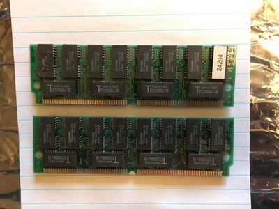
Show full quote
rasz_pl wrote on 2024-01-12, 02:54:
KMM5362000BG build using KM44C1000B http://rfelektronik.se/manuals/Datasheets/KM4 … miconductor.pdf https://datasheetspdf.com/da […]
Show full quote

KMM5362000BG build using KM44C1000B http://rfelektronik.se/manuals/Datasheets/KM4 … miconductor.pdf
https://datasheetspdf.com/datasheet/KMM5362000B2G.html two banks? 4 RAS lines.

KMM5362003BG build using KM44C1000BJ, cant locate datasheet
https://datasheetspdf.com/pdf/542921/SamsungE … s/KMM5362003G/1 one bank? two RAS lines (RAS0 and RAS2).

Different internal organization.

About the chip labelling: KM44C1000B is the generic name, KM44C1000BJ is the specific name for that very chip in a SOJ 26/20 package. There should be no difference in data memory chips. The main difference is that the 2003 module has a single merged parity chip KM44C1003B (no datasheet found) instead of four dedicated single-bit parity chips

Both modules are two banks: The second module uses /RAS2 and RAS3, not RAS0 and RAS2. PS/2 SIMMs have two /RAS lines per bank: /RAS0 and /RAS2 for the primary bank and /RAS1 and /RAS3 for the secondary bank. The reason for two /RAS line is mainly to split the load of driving up to 36 x1 chips. The older modules has 12 chips per bank (8 data chips (4 MBit: 1M x 4), 4 parity chips (1 MBit: 1M x 1), as already mentioned in the thread), whereas the newer module just has 9 chips per bank: 8 data chips in the same way, but only one 4MBit parity chip in a special "one /CAS per bit" configuration. This special parity configuration can cut costs and behaves the same as the 4 individual parity chips in usual circumstances.

A standard PS/2 SIMM memory controller always drives /RAS0 and /RAS2 to the same level, the same is true for /RAS1 and /RAS3. So as long as the drivers are not overloaded, the memory controller doesn't notice which RAM chips are connected to what /RAS line. Having only 9 chips per module allows a single /RAS line to be used without being afraid of overloading a standard PS/2 SIMM mainboard. The incompatibility of the newer SIMM may be rooted in different causes: Possibly this system has weaker drivers and can tolerate 6 chips per /RAS line, but not 9 chips per /RAS line. Another (remote?) possiblity is that this board (didn't look into the technology) tries to use the module as four banks of 16 bits by considering /RAS0 and /RAS2 as /RAS lines for dedicated halves of the first bank. This will work only if the routing of the /RAS lines to the memory chips is split exactly in the way the main board expects - and it will not work at all with the "merged parity chip" design of the later module, because splitting the bank into two x18 halves requires two parity chips connected to /RAS0 and the other two parity chips connected to /RAS2.

Understood, very interesting!
Is there any way to analyze any of this with a scope? Perhaps looking at the RAS lines and accessing the RAM at alternate word addresses?

Reply 21 of 45, by mkarcher

User metadata
Rank l33t
Rank
l33t
Jollyroger wrote on 2024-01-12, 15:22:

Is there any way to analyze any of this with a scope? Perhaps looking at the RAS lines and accessing the RAM at alternate word addresses?

If you have a digital two-channel scope (which I guess you have asking a question like that), I recommend to scope /RAS0 on one channel and /RAS2 on the other channel, and edge trigger on one of the channels. The expectation on a standard memory controller is that /RAS0 and /RAS2 are always at the same level, that means whenever there is a rising / falling edge on /RAS0, there also will be the same kind of edge on /RAS2. You will observe a minimum high time and a minimum low time on /RASx, so no matter what the other circumstances are, you will always find /RAS0 low for a certain time before a rising edge, and always find /RAS0 high for some time after the rising edge. If /RAS2 is equal /RAS0, the same will be true for /RAS2, even if you trigger off /RAS0. And that's where the final idea comes into play: Put the scope into "infinite persistence" mode, so it will show all traces it ever captured overlaying each other. If /RAS0 and /RAS2 are always identical, you will get a pattern like
"XXXX__/~~~XXXX" for both /RAS0 and /RAS2. If you observer /RAS2 being high just before /RAS0 has a rising edge, you know that at this point in time, /RAS2 was different from /RAS0.

Another possiblity would be using X/Y mode, putting /RAS0 on X and /RAS2 on Y. The obeserved patterns should be two intense dots at the end of one diagonal line if /RAS0 and /RAS2 are always driven the same way.

Reply 22 of 45, by Jollyroger

User metadata
Rank Newbie
Rank
Newbie
mkarcher wrote on 2024-01-12, 18:53:
If you have a digital two-channel scope (which I guess you have asking a question like that), I recommend to scope /RAS0 on one […]
Show full quote
Jollyroger wrote on 2024-01-12, 15:22:

Is there any way to analyze any of this with a scope? Perhaps looking at the RAS lines and accessing the RAM at alternate word addresses?

If you have a digital two-channel scope (which I guess you have asking a question like that), I recommend to scope /RAS0 on one channel and /RAS2 on the other channel, and edge trigger on one of the channels. The expectation on a standard memory controller is that /RAS0 and /RAS2 are always at the same level, that means whenever there is a rising / falling edge on /RAS0, there also will be the same kind of edge on /RAS2. You will observe a minimum high time and a minimum low time on /RASx, so no matter what the other circumstances are, you will always find /RAS0 low for a certain time before a rising edge, and always find /RAS0 high for some time after the rising edge. If /RAS2 is equal /RAS0, the same will be true for /RAS2, even if you trigger off /RAS0. And that's where the final idea comes into play: Put the scope into "infinite persistence" mode, so it will show all traces it ever captured overlaying each other. If /RAS0 and /RAS2 are always identical, you will get a pattern like
"XXXX__/~~~XXXX" for both /RAS0 and /RAS2. If you observer /RAS2 being high just before /RAS0 has a rising edge, you know that at this point in time, /RAS2 was different from /RAS0.

Another possiblity would be using X/Y mode, putting /RAS0 on X and /RAS2 on Y. The obeserved patterns should be two intense dots at the end of one diagonal line if /RAS0 and /RAS2 are always driven the same way.

I do have a digital oscilloscope (4 channel), so I may be able to do this (not my everyday thing 😀 )
What is the target of checking the two RAS signals at once? To see if they are all triggered together (hence a single 32 bit bank) or not (two 16 bit banks)?

Reply 23 of 45, by mkarcher

User metadata
Rank l33t
Rank
l33t
Jollyroger wrote on 2024-01-12, 23:30:

What is the target of checking the two RAS signals at once? To see if they are all triggered together (hence a single 32 bit bank) or not (two 16 bit banks)?

Exactly. If the system would do funny things with the two /RAS signals, that would be a good explanation why only few selected module types work with it. There might be lots of other reasons, but that's one you can quite easily verify.

Reply 24 of 45, by Jollyroger

User metadata
Rank Newbie
Rank
Newbie
mkarcher wrote on 2024-01-12, 23:44:
Jollyroger wrote on 2024-01-12, 23:30:

What is the target of checking the two RAS signals at once? To see if they are all triggered together (hence a single 32 bit bank) or not (two 16 bit banks)?

Exactly. If the system would do funny things with the two /RAS signals, that would be a good explanation why only few selected module types work with it. There might be lots of other reasons, but that's one you can quite easily verify.

Gotcha, ok. I will look up the pins locations and set something up to hold the two probes in place. Any recommendations on effective probe holders/placers?

Reply 25 of 45, by pentiumspeed

User metadata
Rank l33t
Rank
l33t

The 12 chips type is to allow using on a 16 bus bit CPU. Good example IBM 50Z and late 386sx machines by IBM and others using 72 pin SIMMs.

Cheers,

Great Northern aka Canada.

Reply 26 of 45, by mkarcher

User metadata
Rank l33t
Rank
l33t
Jollyroger wrote on 2024-01-13, 00:30:

Gotcha, ok. I will look up the pins locations and set something up to hold the two probes in place. Any recommendations on effective probe holders/placers?

I'm afraid, I can't recommend any tool/technique that comes with a standard scope. While the hooks supplied with oscilloscope probes only fit DIP chips, there are small hooks often supplied with logic analyzers that can be clipped on SOIC pins. So unless your board uses a DIP chip to drive the RAS signals, the oscilloscope-supplied hooks won't work.

The two RAS pins are quite close to another, so what I usually do is holding both probes with one hand like chinese chop sticks to the two RAS pins, and use the other hand to push the RUN/PAUSE button on the scope to start sampling only after the probes are placed.

Reply 27 of 45, by rasz_pl

User metadata
Rank l33t
Rank
l33t

EEVblog 1583 - Advanced Oscilloscope Triggering: Glitch/Pulse/Runt/Interval https://www.youtube.com/watch?v=1YK_GlnUlI8

Open Source AT&T Globalyst/NCR/FIC 486-GAC-2 proprietary Cache Module reproduction

Reply 28 of 45, by Jollyroger

User metadata
Rank Newbie
Rank
Newbie
pentiumspeed wrote on 2024-01-13, 00:50:

The 12 chips type is to allow using on a 16 bus bit CPU. Good example IBM 50Z and late 386sx machines by IBM and others using 72 pin SIMMs.

Cheers,

Thanks 😀

Reply 29 of 45, by Jollyroger

User metadata
Rank Newbie
Rank
Newbie
mkarcher wrote on 2024-01-13, 08:42:
Jollyroger wrote on 2024-01-13, 00:30:

Gotcha, ok. I will look up the pins locations and set something up to hold the two probes in place. Any recommendations on effective probe holders/placers?

I'm afraid, I can't recommend any tool/technique that comes with a standard scope. While the hooks supplied with oscilloscope probes only fit DIP chips, there are small hooks often supplied with logic analyzers that can be clipped on SOIC pins. So unless your board uses a DIP chip to drive the RAS signals, the oscilloscope-supplied hooks won't work.

The two RAS pins are quite close to another, so what I usually do is holding both probes with one hand like chinese chop sticks to the two RAS pins, and use the other hand to push the RUN/PAUSE button on the scope to start sampling only after the probes are placed.

Chopstick grip it is then 😀

Reply 30 of 45, by Jollyroger

User metadata
Rank Newbie
Rank
Newbie
rasz_pl wrote on 2024-01-13, 09:20:

EEVblog 1583 - Advanced Oscilloscope Triggering: Glitch/Pulse/Runt/Interval https://www.youtube.com/watch?v=1YK_GlnUlI8

Thanks for the link!

Reply 31 of 45, by Jollyroger

User metadata
Rank Newbie
Rank
Newbie

By the way, if this is indeed the problem, then from the datasheets I think the Toshiba THM362020ASG-70 may work (same 4x CAS configuration instead of the single QuadCAS module).
I ordered a pair, we'll see if it works out, while I master the chopstick-probe grip 😀

Reply 32 of 45, by Horun

User metadata
Rank l33t++
Rank
l33t++

Good ! when I said I had Toshiba tms362020as (8main + 4parity per side) I meant they were THM36202AS (AS tin plated, not ASG gold plated) and by description match the datasheet except chip layout is a bit different.
They do have the presence detect, see the pads/resistor near the 24294 sticker. here is a picture of my pair front/back....

Attachments

  • Img_2617s.jpg
    Filename
    Img_2617s.jpg
    File size
    525.48 KiB
    Views
    446 views
    File license
    Public domain

Hate posting a reply and then have to edit it because it made no sense 😁 First computer was an IBM 3270 workstation with CGA monitor. Stuff: https://archive.org/details/@horun

Reply 33 of 45, by Jollyroger

User metadata
Rank Newbie
Rank
Newbie
Horun wrote on 2024-01-13, 18:12:

Good ! when I said I had Toshiba tms362020as (8main + 4parity per side) I meant they were THM36202AS (AS tin plated, not ASG gold plated) and by description match the datasheet except chip layout is a bit different.
They do have the presence detect, see the pads/resistor near the 24294 sticker. here is a picture of my pair front/back....

Aha! When the ones I got on eBay get here I will test them right away. If they work, I may want to purchase yours too, to have some spare ones...

Reply 34 of 45, by Horun

User metadata
Rank l33t++
Rank
l33t++

Maybe 🤣. Make sure they have the right chips ! I see some on ebay saying 8Mb but are 1mb simms (with tc514256 not tc514400)....

Hate posting a reply and then have to edit it because it made no sense 😁 First computer was an IBM 3270 workstation with CGA monitor. Stuff: https://archive.org/details/@horun

Reply 35 of 45, by Jollyroger

User metadata
Rank Newbie
Rank
Newbie
Horun wrote on 2024-01-13, 19:25:

Maybe 🤣. Make sure they have the right chips ! I see some on ebay saying 8Mb but are 1mb simms (with tc514256 not tc514400)....

Yes, the ones I purchased have the tc514400/tc511000 combo...

Reply 37 of 45, by rasz_pl

User metadata
Rank l33t
Rank
l33t

Fantastic, so fun when forum topics have happy endings 😀
Did you try to measure RAS pins in sim sockets to try and see if /RAS0 and /RAS2 are connected together? I still wonder whats the deal with not supporting SIMMS using only two RAS lines. Imo FPGA should have enough grunt to drive all those chips.

Open Source AT&T Globalyst/NCR/FIC 486-GAC-2 proprietary Cache Module reproduction

Reply 38 of 45, by Horun

User metadata
Rank l33t++
Rank
l33t++

Good job ! Glad you got some that work. May sound strange but can you post a picture of them ? you do not need remove them, just a general close up be ok, am curious of the chip layout.

Hate posting a reply and then have to edit it because it made no sense 😁 First computer was an IBM 3270 workstation with CGA monitor. Stuff: https://archive.org/details/@horun

Reply 39 of 45, by Jollyroger

User metadata
Rank Newbie
Rank
Newbie
rasz_pl wrote on 2024-01-25, 02:28:

Fantastic, so fun when forum topics have happy endings 😀
Did you try to measure RAS pins in sim sockets to try and see if /RAS0 and /RAS2 are connected together? I still wonder whats the deal with not supporting SIMMS using only two RAS lines. Imo FPGA should have enough grunt to drive all those chips.

Oh absolutely, there are lots of unresolved topics out there on the Internet, it's very frustrating when people figure something out but never circle back to tell...
I didn't measure the RAS pins (yet), as first of all I simply wanted to check the functionality of SIMM modules with the exact same number of chips (and RAS/parity connections), and the test with these modules seems to confirm that indeed the system handles differently the quad cas modules instead of the four separate modules for parity.
You are probably right that the FPGA (a venerable Altera EPM7128-10) should have enough capability to drive both configurations, although I wonder if this was a design choice...