Reply 40 of 106, by Chadti99

Rank
Oldbie
- Rank
- Oldbie
Looking sick guys! How do I get one with the more official looking logo?
Looking sick guys! How do I get one with the more official looking logo?
I have some "3Dfx Logo" Kits left i reserved for a other member who did not respond until now..
so if anyone still wants a Kit with 3Dfx Logo, drop me a message.
Otherwise you also can get them on https://www.serdashop.com/3DVideoBridge with legit logo.
https://www.retrokits.de - blog, retro projects, hdd clicker, diy soundcards etc
https://www.retroianer.de - german retro computer board
matze79 wrote on 2021-06-14, 10:26:I have some "3Dfx Logo" Kits left i reserved for a other member who did not respond until now..
so if anyone still wants a Kit with 3Dfx Logo, drop me a message.Otherwise you also can get them on https://www.serdashop.com/3DVideoBridge with legit logo.
Been lurking for a while and was going to order a PCB bridge for my new SLI setup, but you mentioned a few months ago that you still had a few of the newer logo? Is that still the case. I have nostalgia for the newer 3dfx logo as I never used my original Voodoo 2 when the old logo was in use.
Thanks
Edit: Ordered from Serda Shop with the old logo. Still interested if the new logo becomes available.
Hey,
Sedarshop has no stock since a while. Do you still have some, or at least can provide the file so I can directly order one from AISLER ?
Thanks
My Intel SE440BX-2 Intel's website Mirror : Modified to include docs, refs and BIOSes.
Proud owner of a TL866 II
Personal GitHub
Unless I missed them I don’t see the PCB files in this thread I am wanting to make a few adjustments to it before I order some are you willing to share it the kicad files?
Excellent idea by the way I saw one in person and I just have to have some👍
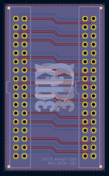
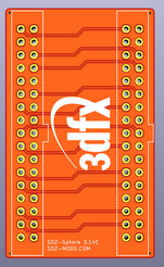
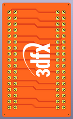
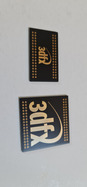
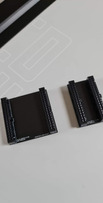
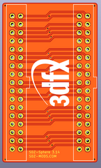
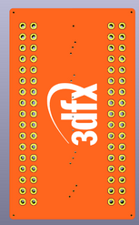
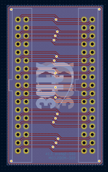
Connectors are 9134-4500PL (black). Gerber files attached for both versions. Use ENIG finish for that bling logo and matte black soldermask.
I'll upload the editable project later today. It's in eagle, but it should import fine in kicad.
Edit: Attached V2_SLI_BRIDGE_V1A_V2A_SCH_PCB.zip containing SCH/PCB.
Sweet! Thanks
Does anyone have a pinout?
I'll upload the PCB project and the schematic. You'll find the pinout there.
Added the files to the previous post. Let me know if you have any problems importing them in kicad.
thanks,
Tried to import it, doesn't seem to be compatible.
That's weird, what kicad version are you using?
Also, what have you tried importing? Vogons says that V2_SLI_BRIDGE_V1A_V2A_SCH_PCB.zip has been downloaded 0 times (not sure how accurate this is). The other 2 archives only contain the gerber files.
that was it, I downloaded the gerber files.
There is a ground plane on the top layer, where the 3dfx logo is (you can check in the gerber files using gerbv). Kicad sometimes has problems importing polygons from eagle.
I got it all figured out started working on it I’m kind of working on it in between things at the moment though somebody mentioned earlier in the thread that they wanted to use the logo from the chips I like it also if someone wants to upload a black and white version of that I can convert it easier in the meantime I’m busy with some other stuff but I can eventually get around to it
It seems that the silk screen logo is the only thing that didn’t translate over But that’s all good, I kind of wanted to use a different logo anyway
The logo is not on the silkscreen, it's on the soldermask layer. It's basically a cutout exposing the gold plated copper.
sdz wrote on 2022-07-11, 18:32:The logo is not on the silkscreen, it's on the soldermask layer. It's basically a cutout exposing the gold plated copper.
Ok, I’m busy on a road trip, so I’m working on it when I can. That explains why I didn’t see it 🤣.
I noticed that one plane was on fbi hsync
was that a conversion error or is there a reason to leave that? I was going to make both planes ground
the mask logo didn't translate over. no biggie 😀
Gerbers/files above^
This was really hard on a laptop with a track pad 🤣, take a look tell me what you think? 😀
I tried to use the other logo but it didn't turn out well. 🙁
which is a bummer because that's the main thing I wanted to change.
but here is what I did:
-moved both planes to ground
-rounded edges
-centered trace steps
-added ground vias
I think it would be cool to attempt bendy/teardrop traces on this.


EDIT:
yeah, looking at this I see you staggered the traces. that's not how it converted over.
I may actually go ahead and stagger them again. lemme take a look. I think that is better.
The FBI hsync plane is an import error, there is only a ground plane in the eagle files.
The GND vias aren't needed, there is a continuous ground plane on the other layer tied to the connector GND pins. Not using vias also looks way better as there are no holes in the logo.
Sadly I don't see how the old logo could be reproduced on a normal PCB, I may try fireing up my laser one of these days and see if something can be done.
In the meantime, the new 3dfx logo in gold looks really nice (the attached picture doesn't do it justice).
Edit:
I don't understand what you mean about the staggered traces, the photo you attached is not my PCB. My design has a continuous reference ground plane and all the signals on the other side.
here is a new version. (staggered traces, one side then the other)
I see now that two people have made the same adapter. Sorry about that confusion.
ultimately it's not much different than your/their design. thanks for letting me play with it.
ah, in gold. is see your point... wow. that would look very nice! Your design would work best for that for sure. it all makes sense why you designed it that way now.