First post, by Thermalwrong
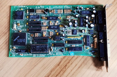
Back in June in the 'what retro stuff' thread, I posted about the CT1350B that I'd got hold of which had its ISA port cut off, here's how it was looking to start with:
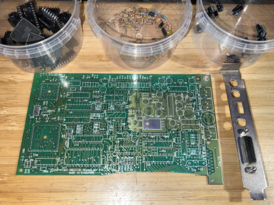
I got it from another collector on thebay but they'd clearly got hold of it from a gold scrapper somehow 😀 The major chips are still there at least.
I could solder / graft on an ISA slot and just use it, but my plan is to get a reproduction PCB made - I'm not the first, chipkin.ru has a reproduction CT1350 PCB, but I wanted to make my own, it's an interesting challenge. I've built one of TubeTime's Snark Barker CT1320 reproduction SB 1.5 cards and made a couple of ISA cards / risers for myself which wor
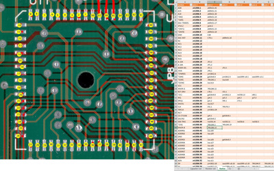
So I thought I'd get started by depopulating the board and measuring the value of every capacitor still present, which was actually pretty much everything, there are 80 capacitors and 51 resistors. Now all recorded in a spreadsheet that I'm using as the working document. That's also got the ICs listed in there because now all the ICs have fallen off:
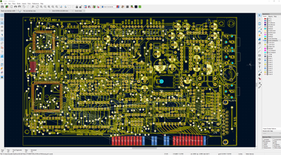
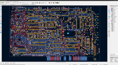
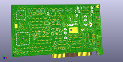
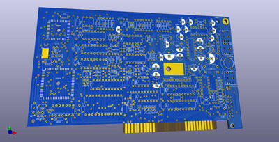
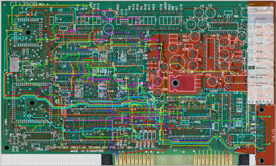
With the PCB depopulated, it could then be scanned with a big 'ol CCD scanner I keep because it does such high res and unlike CMOS scanners, is okay with some depth of field / item distance from glass. The front and rear scans are overlaid since this board has no big ground planes, the lines overlay very nicely and are easy to follow:
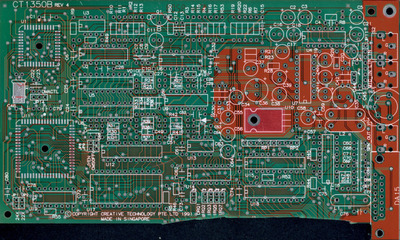
If this was more than a 2 layer board, this part would need to be destructive, but it's not so I'll probably use the original PCB as wall art.
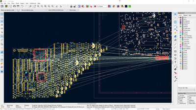
That lead to me making a vector image by tracing the image with Inkscape, which I then imported into KiCAD as the basis for the board / part locations - I was hoping that I could simply make up some components in the PCB and join them up as per the PCB's traces. I got this far, it was looking good:
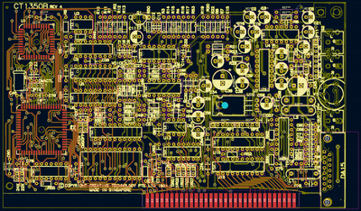
I spent a lot of time on the silkscreen layer, but the noise and high number of vector points resulting from the scan meant that it ended up looking a bit blobby, viewing it on JLC PCB's gerber viewer. But that's easy enough to remake I think.
I had it to the point that most of the front pins were connected up to the pins matching how the original board's traces were.
The further I got, the more I realised that things like minimum trace spacing and design rule checks just weren't going to work right without a schematic. Usually when making a PCB in KiCAD, you'd start from a schematic, generate a netlist and import that into the PCB making tool to determine which parts it has and how they're supposed to link up. But I'd just jumped into the PCB maker. Oh well, it was worth a try.
I have no schematic and it's quite a task to reverse engineer where all the pins go.
So it's sat on the shelf for a few weeks while I avoided looking at it - the path that I think will work is; I need to make a schematic to make the PCB the right way. Without that, there's a possibility of getting boards made with small missed connections here and there, requiring bodges.
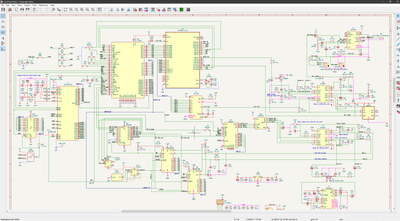
Making the schematic could be tricky because the pinout of the CT1336 isn't listed anywhere or known as far as I'm aware. On the other hand, this is mostly a simplified CT1320 SB 1.5 and there's TubeTime's Snark Barker schematic to refer to, along with the datasheets for all the known parts, so it's possible to work out pretty much everything...
![2022-08-05 22_30_53-_ct1350 [ct1350_] — Schematic Editor.png](./thumbs/37740_362381afeef3044970211b02d5f43ebe/2022-08-05%2022_30_53-_ct1350%20%5Bct1350_%5D%20%E2%80%94%20Schematic%20Editor.png)