They are called blind vias.
I won’t be in front of a computer with kicad again for some days to come. But I will return and will be on here in meanwhile from phone 😀
I am unsure about using v4.0 it seems that you would want the pcb made in the newest version? Not being able to open it on your end, perhaps you have a junk computer you are willing to load up with windows 10/11?
Anyway. Kicad can make a blind via, which is super cool. The problem is that jlc can’t manufacture it.
If you find a manufacturer who can let me know their board setup specifications.
But I think it is a mistake to make the board so specialized. Even though the blind vias is a wonderful idea.
I think SMD or offset is the best option.
This is going to require a lot of layers with offset. Again, we need to do a bunch of drafts to research best routing and see that it is even possible. But with smd, it should be a lot more organized.
It sucks, with smd we are still going to need vias. Next to the smd pads. And with offset we will have two thru hole pads. Which will take up a lot of space.
You keep bringing me bowls of spaghetti to organize 😂🍝
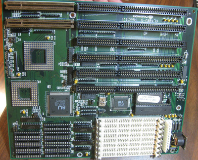
Can we upload high res pics of oem versions to analize?