majestyk wrote on 2022-12-02, 14:39:I found one of my old K6BV3+ /66 the other day that was equipped with just one 1MB cache chip.
I always wanted to upgrade to 2MB […]
Show full quote
I found one of my old K6BV3+ /66 the other day that was equipped with just one 1MB cache chip.
I always wanted to upgrade to 2MB but some component was always missing.
The first step is to solder a second 64x128K chip in it´s place.
The second step is to adjust the jumpering. R145 has to be moved to position R143 and R 137 (or R138) to position R203.
The third step is replacing the TAG RAM:
On 512K or 1MB versions there is a 256K chip (32Kx8, 28 pin SOJ 300 MIL) while 2MB boards have a 512K chip (64Kx8, 32 pin SOJ 300MIL). All chips are 8nS.
These 512K chips were made bei Utron and one more manufacturer and are virtually non-existent today. You will find datasheets but no seller offering them.
That´s why I chose a 1MB chip (128Kx8) 10nS hoping a good sample of a 10nS type today might be as good/fast as a bad sample of a 8nS type back in 1999.
These chips are still available, but you have to make sure they´re 300MIL SOJ and that they have the old pinout with Vss and Vcc at pins 32/16. Modern chips have these pins in the middle of the package due to advantages at high frequencies.
Of course there´s one unused address line in the 1MB chip (A16). This line needs to be grounded, the system won´t work with this pin open. There´s a ground pad nearby so this is no effort.
The attachment TAG_mod.JPG is no longer available
I still have to test this setup to make sure there are no instabilities at 100MHz FSB.
The FIC VA-503+ has 1MB L2 cache and two 512K chips. The TAG RAM is 256K and the layout only provides the 28 landings for this chip.
I have repeatedly read in online boards that there is a "rare 2MB version" of this model. I doubt this ever exixted due to the TAG limitation.
I tested this setup with both 256MB and 512MB RAM:
In the 256MB case all 256MB are being cached in "Write Back" mode, "Write Allocation" gets enabled by BIOS.
If there´s 512MB RAM present, 512Mb are being cached, but BIOS switches to "Write Through" mode to avoid half of the RAM being uncached. Write Allocation is disabled in this case.
Th data from the table of cacheable areas (see above) is correct as we see.
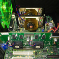
And here´s a picture of the finished product:
The attachment k6bv3plus66_total1.JPG is no longer available
Thank you for sharing this information here on vogons. I found this by coincidence.
As I have two identical such boards - one equipped with 1 MB of L2, and another one equipped with 2 MB of L2, so they can be compared regarding the resistors for enabling the second module of 1 MB to reach a total of 2 MB.
Both boards are in original condition: NO hardware-modding on them by myself.
Yes, you are right about the TAG-RAM for the 2-MB-version: on my board, there is a 128Kx8-chip having 10 ns, and it works perfect 😀
Your info about R111, R112, R113 is correct, too.
BUT, R129 and R133 DO NOT NEED to be replaced (= less soldering work), at least for an upgrade from 1 MB to 2 MB L2!
As I do not have a board with 512 KB L2, I can not see, if R130 and R134 are present (instead of R129 and R133), or not.
I use my 2-MB-board with WinXP and a K6-2+ 533 @ 600 MHz (2,4 VCore/FSB 100 MHz) and 512 MB RAM with no problems.
They are still 2 inaccuracies:
- Cachecheck in DOS always means, there are 64 MB of RAM present
- CPU-Z in Windows means, the RAM is running at CL3 (although CL2 set in BIOS)
Also, I have a question- what software are you using to check what you wrote above "In the 256MB case all 256MB are being cached in "Write Back" mode, "Write Allocation" gets enabled by BIOS.
If there´s 512MB RAM present, 512Mb are being cached, but BIOS switches to "Write Through" mode to avoid half of the RAM being uncached. Write Allocation is disabled in this case."
I LOVE CPUs RUNNING IN [GonzoHz]