First post, by SergeK

- Rank
- Newbie
Hi,
I am working on a 386SX/486DLC motherboard based on the SARC RC2016A chipset (https://github.com/skiselev/mb386sx-rc2016).
It started out of curiosity of reverse-engineering the schematic using the Marco Both's M369F replica PCB layout (https://github.com/Marco-Both/M396F-Replika)
Eventually I made a few improvements, and as of now (version 2.3) the board is pretty much ready. I tested the previous version, and fixed one schematic bug that prevented it from booting.
I've done some experiments on my board, and I have some questions.
TI486SXLC2-50 Clock Doubling
I wanted to get the clock doubling working with a TI486SXLC2-50 CPU. This processor and others I tested - Intel 386SX-33, TX486SLC-33, run fine on 20, 25, 33, and 40 MHz. The latter two get a bit warmer, but, being 5V parts, this is expected.
I run TI486SXLC2-50 at 3.3V voltage using this adapter: https://github.com/skiselev/i386sx-socket
To enabled double clocking, I ran the system at either 20 or 25 MHz (CLK2 = 40 MHz or 50 MHz), and I tried flipping bit 6 - clock doubling enable of CCR0 / 0xC0 (Configuration Control Register 0) using something like this:
MOV AL,0C0h
OUT 22h,AL
IN AL,23h
OR AL,40h
MOV AH,AL
MOV AL,0C0h
OUT 22h,AL
MOV AL,AH
OUT 23h,AL
(optional delays, writing POST port 0x80, etc.)
INT 20h
The system hangs after running this code... Not completely... I still see activity on ISA bus and CPU, it just does something non-deterministic, if I had to guess.
I tried adding a delay after this sequence, e.g., a loop with writing to I/O port 80h (POST port), and in this case, the loop runs fine, and I can see numbers on the POST card. But as soon as the program exists, the system hangs.
So there must be something that breaks... maybe from the DOS, I/O, or memory perspective (assuming that the sequence above runs from the cache... although I can try disabling the cache, and checking if the behavior remains).
Any ideas where to look?
SARC RC2016A5 Chipset and BIOS Support
There are several BIOS versions for SARC RC2016 based motherboards floating around. Generally speaking they are mostly AMI 5.20, and one of the boards used Award 4.50. I find the latter one a bit more user friendly, especially that I can customize it using MODBIN.
Now, some of these BIOSes have chipset settings (some don't). Particularly for this chipset the following:
- ROM Shadowing - this seems to work fine, and I think I identified the chipset configuration registers bits responsible for it. There are two bits for each 16 KiB block at 0xC000-0xEFFFF. I suspect that one means read from ROM write to RAM and another is RAM write protect. I still need to verify that.
- Fast reset/Fast A20 - I still have to test the register 0x92 function. At least with one BIOS, HIMEM.SYS fails to enable A20 when Fast A20 option is enabled.
- Memory parity checking - Some BIOSes have enable/disable setting. I didn't notice any changes in any chipset configuration registers or in 0x61. I tried using SIMMs with and without parity. I don't have a defective SIMM to test. With that said, it appears that chipset does activate the data parity signals going to DRAM regardless of the parity checking setting.
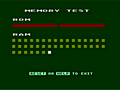
- DRAM refresh rate/burst - Seems to work as expected, although, somewhat counterintuitively, the higher the rate, the slower is the refresh. The rate is actually a divider for the refresh cycle clock... With the rate set to 1, the refresh cycles happen every 15 us (I believe this is the standard/typical period obtained by dividing 14.31818 MHz by 12 before feeding it to the PIT channel 1, and then channel 1 is configured as a clock divider by 18, resulting in 66.28787 kHz refresh frequency). The period is multiplied (and the frequency is divided) by the rate setting, that is, setting the rate to 8, results in ~120 us refresh period or ~8.28598 kHz refresh frequency. The burst setting simply specifies the number of DRAM rows refreshed during each refresh period (1 to 4). The end result is that slowest refresh (and the least impact on the system performance) is achieved using refresh rate of 8 and burst of 1. This seems to work fine with the SIMMs I have.
- DRAM wait states - The setting is either 0 or 1. This seem have almost no impact on performance... The difference that I see in System Speed Test Ver 4.78 is about 0.06% in video memory accesses and 0.03% in CPU cache accesses (why CPU cache is affected?!)
- RAS to CAS delay - Does not seem to impact the performance, but the system hangs after POST if it set to 6. (Works fine with 2 or 4). I'll hook up the scope to see if there are any differences in the delay...
- RAS precharge - Also does not seem to impact the performance. Same, I need to hook up the scope and check.
- IO Channel refresh - This enabled or disables refresh cycles on ISA bus. I suspect the refresh cycles might be needed by some DRAM-based ISA memory expansion boards... Disabling this setting turns off generating refresh cycles - ISA /REFRESH won't pulse, and it slightly improves the performance.
- ATBUS (or AT BUS) stepping - Disabling this seem to add some jitter on I/O and slightly improves the I/O performance. E.g., in the System Speed Test, with this setting enabled, the read rates look very flat given that I use an IDE disk-on-module. With this setting disabled, I get slightly higher read rates, but also some variability between minimal and maximal read speed. Any idea what this setting is supposed to do?
Any insights, comments, or suggestions on what else to test are appreciated.
Thanks,
Sergey
P.S. Here is my reverse-engineered SARC RC2016A chipset documentation: https://github.com/skiselev/mb386sx-rc2016/bl … /SARC_RC2016.md