@Anonymouse Coward
What symptoms do you receive at 2x66? What voltage are you supplying? Your problems may be entirely thermal.
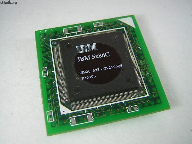
Cyrix/IBM 5x86 Thermal Considerations
As a bedtime story, I've been reading thru some of the old IBM 5x86C thermal literature. I beleive most or all instability associated with the IBM/Cyrix 5x86 series is due to extreme thermal sensitivity above the rated voltage. Even 0.1 V differance seems to have a noticable impact. I've even starting to wonder if branch prediction on S0R5 processors is thermally related as well.
For example, with my 2x66 133 MHz IBM 5x86C, I can have branch prediction enabled and am able to run all of the U4BC Windows benchmarks if the CPU hasn't been turned on for very long. If it is on for more than about 10-20 min., select benchmark tests will crash (noteably test #58-64) with BTB enabled.
DOS branch prediction has always been stable for me on S0R5 chips with BTB and RSTK enabled, and LOOP disabled. In fact, if the CPU isn't on for too long, I can run the U4BC Windows tests with BTB and RSTK enabled. Note that for S1R3 chips, BTB is more successful with RSTK disabled.
Once I've updated the U4BC, I'm planning on soldering on a 5K multi-turn variable resistor to the 4V jumper voltage regulator on the MB8433-UUD. This will enable me to set anywhere from 0-5V to the CPU with great precision. It is my aim to narrow in on an optimal voltage to run these chips at to enable stable operation.
Custom PLL Interposer for Cyrix/IBM 5x86
As for the 1.33X PLL interposer... what we'd really like to do is leave the Cyrix on 2X or 3X. This means that,
33.33 MHz x 1.33 x 3 = 133.33 MHz
33.33 MHz x 2.00 x 2 = 133.33 MHz
40 MHz x 1.11 x 3 = 133.33 MHz
40 MHz x 1.66 x 2 = 133.33 MHz
2 and 3 are the motherboard's CLKMUL jumper; 33.33 and 40 are the motherboard FSB setting, and the other decimal is the desired PLL clock multiplier.
So for ease of use, we need a PLL that can do any one of these:
1.33x, or 2.0x, or 1.11x, or 1.66x. In PLL terms, that works out to 1:4/3, 1:2/1, 1:10/9, or 1:5/3. Rearrange, 4:3, 1:2, 9:10, or 3:5.
So let's see, how about setting the system up for a 66 Mhz CPU (2x33) and multiplying by 2.0? A 1:2 PLL is very common. So let's look again at all our requirements for this PLL,
3 - 5.5 V range
200 MHz max - I figure 200 MHz is a good limit, and will allow for AMD X5-200's
1:2 multiplier
This leaves 3 readily available options,
ICS512MLFT $3.49
ICS512MLF $3.08
NB3N502DG (190 MHz only, but it can also divide clocks) $3.74
That is the cheap part of the project, the expensive part is a PCB interposer prototype. In Canada, I've had some single units made for around ~$1000 each, but people have been shifting towards China. They will do a prototype for $300, inclusive of shipping. Once funding has been acquired, then the circuit simulation can begin. Once a simulated circuit is successful, its time for a benchtop breadboard-like setup. I have found that the simulation model can be overly simplistic and a lot more work need be done at the benchtop stage. Once the benchtop stage is confirmed, i.e. with an oscilliscope, PCB layout can begin. Once this is confirmed, it need be sent off to the "overseas printer". At this stage, it is sometimes needed to re-route wires depending on the complexity, cost, and if a 3D PCB is required.
Is there sufficient demand here to pursue this?
Long story short, it is not a quick job for the home retro hobbiest, nor would it be cheap. It may be possible to hack the gainbery interposer with an external 1:2 PLL, having ghetto wires going everywhere. With my next digikey order, I'll add one of the above mentioned 1:2 PLL's. Although it is SMD, I've had some patient success soldering to an SOIC package. I do have some 1:4 PLL's at home, but they are not rated above 18 MHz.
If somebody knows of an existing interposer with a 2x, 1.33x, 1.66x, or 1.11x PLL onboard, please let me know so that I can have a look at 'em.
@Anonymous Coward
Where did you get the interposer with the 386 PLL? Do you have any socket 3 interposers with frequency manipulation onboard? If so, which ones and where did you find 'em? I figure any socket 3 interposer containing a PGA AMD X5 that was focused on updgrading early 486 DX-33/DX2-66 motherboards must have a 2x or 1.33x PLL on board. Perhaps this is the way to go, google/ebay searching.
EDIT1: I managed to slap 2 of NB3N502DG onto an existing backorder I had with futureelectronics.com Unfortunately, they did not have ICS512MLF. FYI, Future Electronics and Mouser Electronics are often significantly cheaper than Digikey.
EDIT2: An interposer board may not be required. I've found a very suitable location on the Biostar motherboard where the PLL can be inserted. The surface mount resistor, R79, can be desoldered and connected into the ICS512 multipler PLL circuit. The path can then be reconnected through the other R79 solder pad. Alternately, a jumper block or SPDT switch can be used to switch between this extra 2X PLL or not using it. This is now a very simple operation. The ICS512 is convenient in that at 2X, you just leave the selector pins floating! It becomes as simple as connecting 5V, GND, Clock IN and Clock OUT. Just add a decouling capacitor (0.01 uF) between 5 V and GND, and a 33-ohm terminating resistor.