First post, by appiah4

Rank
l33t++
- Rank
- l33t++
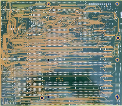
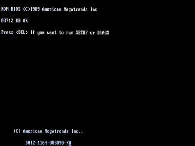
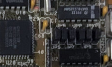
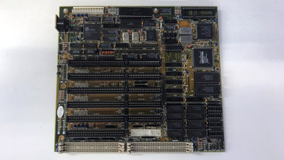
I'm currently working on repairing this 286 motherboard and having some documentation would be nice. Unfortunately there are absolutely zero markings on it. Does anyone know what this motherboard is?
I've tried the regular sites and found nothing..
Attachments
Retronautics: A digital gallery of my retro computers, hardware and projects.