Aaron707 wrote on 2022-12-12, 18:51:
What are dimensions of 2.0 PCB? Pic?
The prototype board is 100x100 mm. It has two additional daughter boards on the top side, a tiny HIDman implementation and a Wemos D1 Mini (ESP8266). I'm currently testing the HIDman, haven't gotten to the modem/ethernet over wifi stuff yet. If all turns out well, I should be able to get everything down to about 100x77 mm, but not sure if it's worth another spin. Might keep the prototype form factor.
I'll post pictures when I've soldered everything together, just playing with the USB HID stuff for now.
Edit: oooh, and I forgot to mention - almost all components, both smd and tht, both sides, are soldered by JLC now. That is very nice for someone who doesn't exactly love soldering. 😀
Aaron707 wrote on 2022-12-12, 18:51:
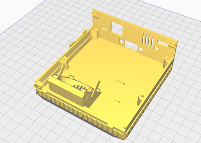
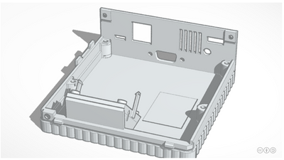
I printed a bottom and finished designing a top. Bottom was good, but needed some changes. Once I soldered my pcb and components some of the bottom capacitors and pins were hitting the standoffs. Going to test my board next then print the case again.
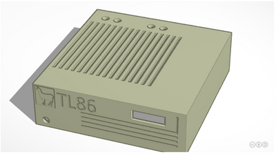
That looks soooo good! 😁 What CAD software are you using? I wanna make one when you're finished! Just gotta find a filament with the proper oldskool beige color! 😉