retardware wrote on 2021-09-27, 02:19:
I guess Intel got much bad feedback from the big OEMs and thus quickly abandoned the slot nonsense for Socket 370.
Sorry, I have to contradict you.
There were several technical troubles that lead to the solution with the slot CPUs.
Please ready my text to understand the die shrinks.
There was a need to integrate more L2 on the processor to improve the performance over the super 7 socket.
There was not enough space on the die to integrate such a big L2.
The first pentium 2 processors were Klamaths in 0,35 micron technology. The die size was 203 mm² with 7,5 million transistors.
After the die shrink to a Deschutes in 0,25 micron its size was 131 mm² (later optimizations led to 118 mm²) with same 7,5 million transistors.
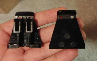
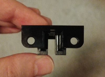
At least Klamath's die size was too big to integrate transistors for a L2 cache. But external L2 over the CPU pins would have been to slow. Intel's solution was the slot 1 interposer that had an extra bus from the CPU to the cache modules. This gave a huge performance boost over the former socket architectures. However, at this time existing cache modules for the interposer were not fast enough. They never got over 350 MHz, so the clock had to be divided by 2 or 3 to the CPU die.
Next evolution was the Katmai in same 0,25 micron technology. It was a 128 mm² die with 9,5 million transistors. It's new KNI/SSE instruction set increased the performance but needed an amount of new transistors.Still remember, overclocking former slot CPUs with cache on the interposer was not that easy because the L2 modules already were running near their border.
However, it's time to watch the Celeron processors now. Intel tried to get rid of the external L2 cache. Intels first try was the not so famous Covington Celeron without any L2 cache. It was easily to overclock it from FSB 66 to FSB 100 and more. But without L2 it lacked so much speed that it fell back behind even the P200 chips. While Covington still was a 0,25 micron Deschutes without L2 it's die size was 118 mm² with 7,5 million transistors.
Intel tried the same thing with the Mendocino Celeron. But the integration of 128 KB L2 in the same 0,25 micron process led to an increment to 19,2 million transistors at 154 mm². Just try to imagine, half of the transistors just for the L2! Since it was integrated on die, it run with full speed without any divider.
Marketed with 300 MHz with 66 FSB it was too easy to overclock the Mendocino Celeron to 450 MHz at 100 FSB. It was the fastest processor at this time then, even faster than the 500 MHz Katmai with its quad size 512 KB L2 cache.
This was the future and the unification of the Katmai and Mendocino lines lead to the Coppermine architecture, and the die shrink to 0,18 micron made it possible to intregrate a bigger L2 cache.
With the integration of the L2 cache into the die its total capacity was halfed from Katmais 512 KB to Coppermines 256 KB. However the gains of the architecturial integration benefits were much larger than losing 50 % of its naked size.
Since so many mainboards and so many of Intels famous 440 BX chipset sold, there were so high demands from the market to continue the production of the CPUs in slot case for still a long time although they did not contain discrete cache anymore.
However, there was a demand for cheaper and smaller mainboards, so Intel developed the socket 370 - and this is where my story ends.