Blavius wrote on 2022-09-15, 07:26:
feipoa wrote on 2022-09-14, 20:48:
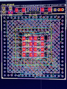
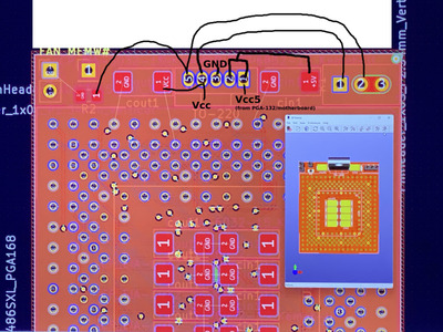
What we definitely want to get rid of is JP1. VCC5 should always be 5 V, regardless of the version of SXL CPU used. I can see people confusing JP1 for bypassing the VRM, which it does not do.
I agree the naming is confusing and we need to solve that. But the voltage on pin J1 of the processor is something we have to be clear on. There is a difference between SXL versions here. According to the manual; for all SXL processors (including the one you intend to use) pin J1 needs to be VCC3 - NOT VCC5! ....BUT, for the 'G' variants of the processor pin J1 needs to be VCC5. Now these seem to be rare (never seen a picture), so you could argue not to bother with them, and the associated jumper.
Blavius, I'm not sure what these non-G variant 3.x volt SXL2 chips are. You may have a typo in your above statement. You've said that the processor I intend to use requires J1 set to VCC3. However, we are using the G variant in this upgrade, as shown in previous posts.
I have a QFP144 SXL2-66 3.6V with part number TI486SXL2-G66-HBN on a commercial adapter. VCC5 (J1) is set to 5 V on this unit (measured with DMM). The 3.6V chip intended for the adapter at hand now has part number TI486SXL2-G66-GA. Both these are G variants.
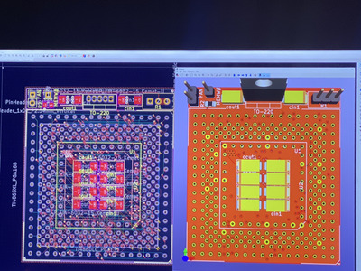
QFP144 photo: download/file.php?id=43455&mode=view
PGA168 photo (to be used in this adapter): download/file.php?id=43454&mode=view
Manual states, "This pin is VCC5 for the T1486SXL-G40 and TI486SXL2-G50. It is VCC for all other devices." Thus we should eliminate JP1.
Sphere: I will need to do some desolder to get a better measurement, but will get it done.
Sphere478 wrote on 2022-09-15, 07:30:
Btw, can you give measurements in thousands of inch, switching back and forth between metric and imperial causes small errors. So I have been converting your measurements on google. :-)
Lol! I was wondering how on earth you are using inches for these measurements - it seems so unnatural to me.
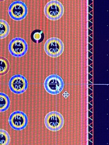
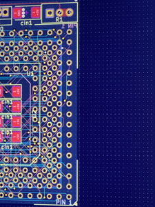
Regarding the VCC5 pin, which is location J1 on the PGA-168 grid, this pin should go permanently to 5 V, not VCC3. See discussion above.
Regarding traces for VRM, trimmer, etc, it should be the same as what's on Blavius' layout, with his R1 resistor going to pins 1 & 2 of the trim pot.
Plan your life wisely, you'll be dead before you know it.