feipoa wrote on 2022-10-01, 11:30:Looks nice. Hope it works. Are you expecting me to go one-by-one on each trace again? That was rather painful on the eyes the la […]
Show full quote
Looks nice. Hope it works. Are you expecting me to go one-by-one on each trace again? That was rather painful on the eyes the last time I did this.
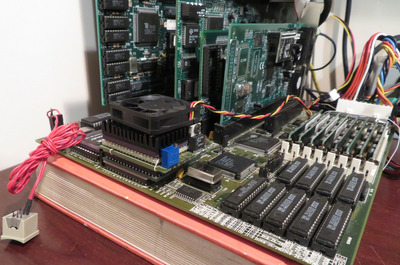
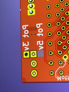
I can try J1 on Vcc3, but I think the chance that this is the problem is slim. I'm also not able to get my original prototype working on the same motherboard I showed in earlier posts that it worked. Re: Custom interposer module for TI486SXL2-66 PGA168 to PGA132 - HELP! I will probably need to check each pin one by one. My prototype had J1 on 5V for the SXL2-G66 CPU. I will also need to hunt down the same ISA cards shown in that photo. Maybe even the same memory sticks.
I also tried running the adapter with a 5V SXL2-50 rather than the G66 chip, but issue was the same. I upped the voltage to 4.8 V using the trimmer when using the 5V SXL2 chip. I will need to spend more time with this. It will probably take a week or two.
I tested the G66 CPUs in my other adapter, so I know they work.
EDIT: Yes, I checked the voltage to the CPU. I attached leads to the Vcc and Vss pins on the PGA168 CPU that were furthest from the VRM and I measured 3.60 V. I also measured 5.02 V to the VRM's input.
EDIT2: Thinking back 5 years, I do recall this board being finicky with SXL chips, like the ISA cards would only work in particular slots on the ISA bus.
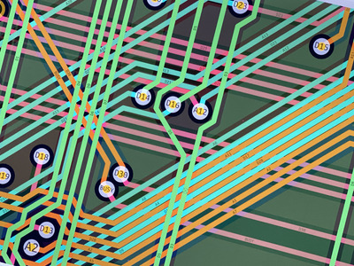
The nets haven’t changed. So they should all be going to the same places. One would imagine re checking wouldn’t be needed. As the program gives me a line for each net. It is probably sufficient that you checked those on the previous version.
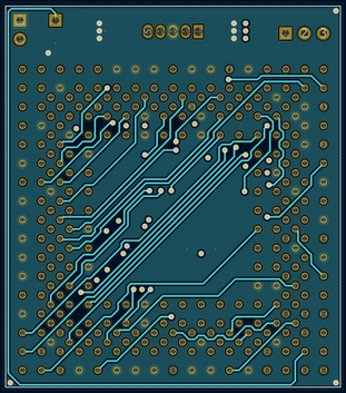
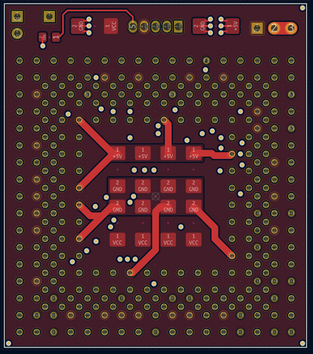
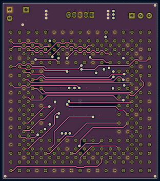
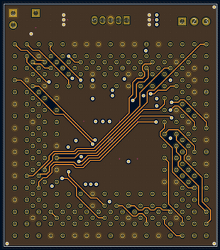
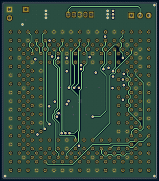
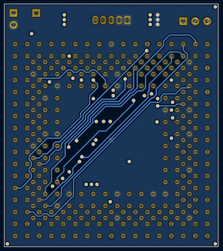
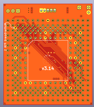
I’m bummed that I wasn’t able to get more isolation on the trace runs or equal length. But this is just what we are gonna have to do as the other ideas didn’t work out. If I do equal length we will loose all sorts of ground plane conductivity. And route traces by all sorts of interfering signals. Worse so than it already is.
I was at least able to minimize vias on this version and make traces larger.
The power planes look really good also.
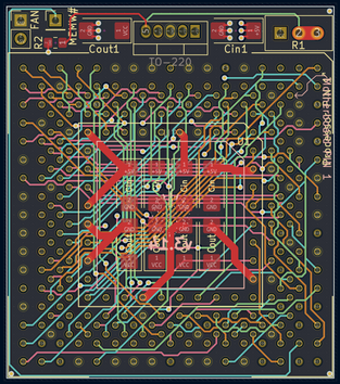
So maybe one more beta and prototype it.
I’m hoping others can take a look and make suggestions for the next beta though, pool our brainpower, try out inprovments/ideas.
I think we have something pretty close to the best possible thru hole design here.
A smd version may be able to do better.
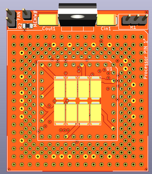
Soon it will be on you to solder this thing. 😀 hope you are successful. Doesn’t look fun.