VOGONS


Information request for SMC I/O card

Topic actions

Reply 20 of 35, by eesz34

User metadata
Rank Member
Rank
Member
Horun wrote on 2023-03-26, 03:49:

If you figure out where they go/what they do and post it here will add it (with your picture, the text, the datasheet, the schems) to our driver library with creds to you, PC Hoarder and a link to here for the work involved if that is ok.

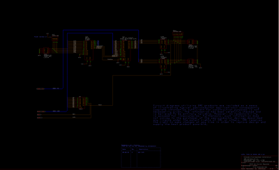
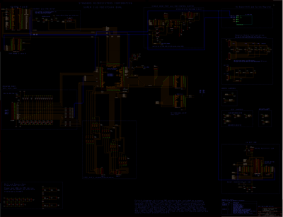
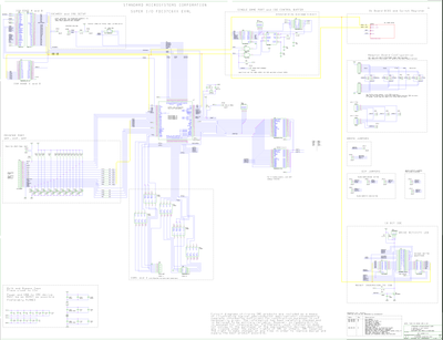
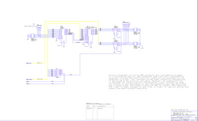
I think I have this figured out. First, I pieced together screenshots out of OrCAD since I can't figure out another way. Given this is a 30 year old DOS program, there probably isn't. It looks like the BIOS schematic got recompressed by the website. I'll have to see what if any noticeable effect it has on the readability.

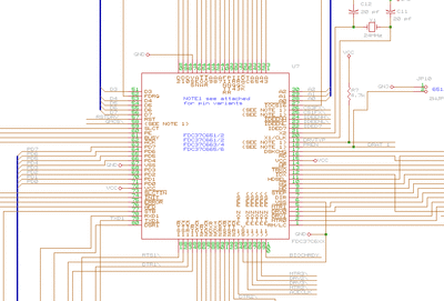
All the headers and jumpers are in the schematics, and most are in the jumper text file. Some notes:
-JP25 and JP26 appear to be some sort of configuration that the BIOS would read. Since mine doesn't have a BIOS and I'm not sure if there is one available, they are simply not used.
-The board has a JP28, but there is no JP28 in either schematic. JP28 is actually JP26 on the main schematic. The schematic states it's an IRQ pull-up for motherboards that don't have it. I don't see an issue enabling this if you're not sure as it's only 4.7K.

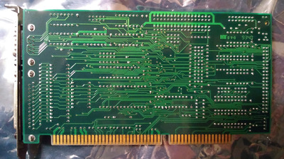
Again big thanks to PC Hoarder Patrol. Having this documentation for this apparently uncommon card is infinitely helpful.

Attachments

  • SIO6XXE2.png
    Filename
    SIO6XXE2.png
    File size
    60.24 KiB
    Views
    508 views
    File comment
    BIOS schematic
    File license
    Public domain
  • SIO6XXE1.png
    Filename
    SIO6XXE1.png
    File size
    389.48 KiB
    Views
    508 views
    File comment
    Main schematic
    File license
    Public domain

Reply 21 of 35, by Horun

User metadata
Rank l33t++
Rank
l33t++

Nice thanks. Ha there are two JP26 (the 8 pin header and the actual two pin jumper). Your pics are great but am used to white background for Schems so edited them to grey scale (probably not the best choices for palette)...
might work on it a bit...

Hate posting a reply and then have to edit it because it made no sense 😁 First computer was an IBM 3270 workstation with CGA monitor. Stuff: https://archive.org/details/@horun

Reply 22 of 35, by eesz34

User metadata
Rank Member
Rank
Member
Horun wrote on 2023-03-28, 06:14:

Nice thanks. Ha there are two JP26 (the 8 pin header and the actual two pin jumper). Your pics are great but am used to white background for Schems so edited them to grey scale (probably not the best choices for palette)...
might work on it a bit...

Right, they have a JP26 in each SCH so it wasn't caught by the schematic capture. I can't find a way to change the background.

I've also attached the rear side. Look at the ISA connector on the 8-bit section for a surprise. Very odd trace there....

I was just thinking, are you interested at all in the PCem drive image? It's all set up and ready to go with OrCAD and a video driver to 1024/768. No big deal either way.

Attachments

Reply 23 of 35, by weedeewee

User metadata
Rank l33t
Rank
l33t

From what I can gather, none of the missing chips are required for the card to work.

or maybe U6 is required for address decoding ?

Right to repair is fundamental. You own it, you're allowed to fix it.
How To Ask Questions The Smart Way
Do not ask Why !
https://www.vogonswiki.com/index.php/Serial_port

Reply 24 of 35, by eesz34

User metadata
Rank Member
Rank
Member
weedeewee wrote on 2023-03-28, 16:01:

From what I can gather, none of the missing chips are required for the card to work.

or maybe U6 is required for address decoding ?

U6 appears to be for address decoding, but only to read the set of jumpers on JP25 and JP26. I have not yet tried it on a motherboard, but will eventually. It looks nearly new with no use marks on the bracket or external connectors at all, so I'm hopeful.

Reply 25 of 35, by Horun

User metadata
Rank l33t++
Rank
l33t++

Yeah agree those are only if a BIOS is being used. Here are the reversed color schematics..

Attachments

Hate posting a reply and then have to edit it because it made no sense 😁 First computer was an IBM 3270 workstation with CGA monitor. Stuff: https://archive.org/details/@horun

Reply 26 of 35, by eesz34

User metadata
Rank Member
Rank
Member
Horun wrote on 2023-03-29, 00:18:

Yeah agree those are only if a BIOS is being used. Here are the reversed color schematics..

That's impressive. Did you have to pour white on all the black areas? I wouldn't know how else to do it.

Also I just noticed a mouse pointer in the upper right of the main schematic that I forgot to delete 😀

Reply 27 of 35, by rasz_pl

User metadata
Rank l33t
Rank
l33t
eesz34 wrote on 2023-03-29, 02:05:

That's impressive. Did you have to pour white on all the black areas? I wouldn't know how else to do it.

Irfanview
-click I for picture information and check number of individual colors
-reduce number of colors to that number
-edit palette, in this case first color is black and just changing it to white is good enough, but OP changed track and annotation too for even easier readability

Attachments

Open Source AT&T Globalyst/NCR/FIC 486-GAC-2 proprietary Cache Module reproduction

Reply 28 of 35, by eesz34

User metadata
Rank Member
Rank
Member
rasz_pl wrote on 2023-03-29, 10:22:
Irfanview -click I for picture information and check number of individual colors -reduce number of colors to that number -edit p […]
Show full quote
eesz34 wrote on 2023-03-29, 02:05:

That's impressive. Did you have to pour white on all the black areas? I wouldn't know how else to do it.

Irfanview
-click I for picture information and check number of individual colors
-reduce number of colors to that number
-edit palette, in this case first color is black and just changing it to white is good enough, but OP changed track and annotation too for even easier readability

Oh ok that makes sense. I obviously know nothing about editing images 🤣

Reply 29 of 35, by Horun

User metadata
Rank l33t++
Rank
l33t++

Yep that is basically what I did but used old Paint Shop Pro 6 on the old box.

Hate posting a reply and then have to edit it because it made no sense 😁 First computer was an IBM 3270 workstation with CGA monitor. Stuff: https://archive.org/details/@horun

Reply 30 of 35, by eesz34

User metadata
Rank Member
Rank
Member

An update for anyone who might run across one of these and find this thread. The card works great, but the jumpers text file isn't completely accurate. They have some of the jumper positions swapped, specifically the IDE and floppy I/O address. So I'd encourage anyone who has one of these and trying to get it to work to look at the schematic and datasheet first. (and does anyone else have one of these? They seem very rare)

Reply 32 of 35, by eesz34

User metadata
Rank Member
Rank
Member
ForzaLaVida wrote on 2023-05-28, 17:54:

Any chance you could try to open a very old OrCAD schematic for me?

https://drive.google.com/file/d/1llsoXPjLP-Hl … iew?usp=sharing

Much appreciated.

I will try it, tomorrow I'm hoping.

Reply 33 of 35, by eesz34

User metadata
Rank Member
Rank
Member
ForzaLaVida wrote on 2023-05-28, 17:54:

Any chance you could try to open a very old OrCAD schematic for me?

https://drive.google.com/file/d/1llsoXPjLP-Hl … iew?usp=sharing

Much appreciated.

Doesn't open with OrCAD 4.20, but the header of the file looks pretty similar to the one I dealt with. Any idea what this was drawn in?

Reply 35 of 35, by eesz34

User metadata
Rank Member
Rank
Member
ForzaLaVida wrote on 2023-06-04, 20:41:

Likely a version from 88/89 best guess. Though I have located a copy of that schematic, I'm still curious about that orcad version

The only way you could determine that I suppose would be to install progressively higher versions of OrCAD until it opens it, assuming it is OrCAD. The schematic I wanted to open that is the subject of this thread luckily had text in it announcing that it was OrCAD 4.20, but that's only because the drafter put it there.