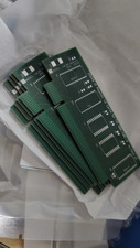
I have chips for three modules coming, and then 5 PCBs. So if someone has a system, and needs one, there is a chance, but first we gotta see if it works at all 😁
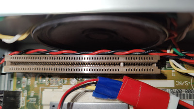
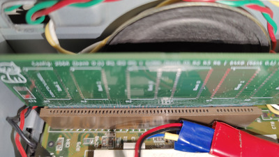
On my Globalyst 510, the 'vlb' socket is in no way under the floppy drive, so clearance was not an issue
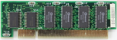
Globalyst 575 has the same mainboard as Globalyst 550 (not made by FIC). It has the 2nd version of the VLB-cache-stick that I showed some posts earlier.
Globalyst 575 has the same mainboard as Globalyst 550 (not made by FIC). It has the 2nd version of the VLB-cache-stick that I showed some posts earlier.
ATT-Globalyst_550_575.jpg
You mentioned it, but I dont remember seeing this picture. Could you please link/post back side too? Do you happen to know the model of mobo in 550? nvm found it https://theretroweb.com/motherboards/s/atandt … globalyst-550-c interestingly documentation calls cache slot SL2 there, while GAC-2 calls it SL1 so they did mark it differently so no one makes the mistake of plugging wrong Cache module :---)
Last edited by rasz_pl on 2024-02-19, 17:01. Edited 1 time in total.
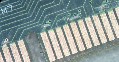
Looks like the fingers are covered in mask 🫤
Looking back at the renders, the fingers are under the mask there too... Oops, looks like we all missed that little detail 🫣
Width seems ok, but it's too thick as it is to be able to push it down in the slot
Looks like the fingers are covered in mask
Looking back at the renders, the fingers are under the mask there too... Oops, looks like we all missed that little detail 🫣
we all looked at it and went yes that looks perfectly normal 🤣 at least thats what I tell myself to deflect some of the blame 😜
Mask cutout missing on all Edge Connector pads 😳
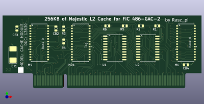
Now that Im having a second look CT cap footprints might be too large, those were provisioned for big tantalums, are the caps you bought fitting fine in there?
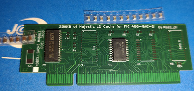
Are SOJ SRAM footprints ok? Pads look awfully small to me 😀
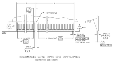
Im not loving edge connector middle gap being this wide, leaves possibility of bad alignment 🙁 I think I used this https://www.eevblog.com/forum/vintage-computi … 450/#msg3592450
but not sure if I followed it to the letter, I remember fiddling with it, measuring ... mine is even smaller than this drawing 😒 1.805 while drawing demands 1.86-1.96 I think I measured original PCI slot gap and it was way smaller than this so I made mine somewhere in between. Ill change final project to tighter PCI gap, VESA VLB technical docs be damned.
Width seems ok, but it's too thick as it is to be able to push it down in the slot
Will have to see what can be done to get the fingers exposed and make it go in the slot.
VLB slots are very tight, extra mask will definitely exacerbate it. Beveling will also help. I read n some PCIE card github suggestion to make yourself a 45 degree jig before sanding for that perfect even angle 😀
Regarding the divider, I would not suggest making it smaller, as it appears to get wider as you go deeper in to the slot, and I think it's about right (non scientific assessment)
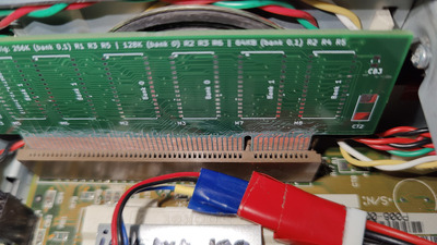
After much sanding, the board just about goes in, but I would describe it as nearly a death grip. You have to see saw it in, as if you try and push it straight down, it refuses to go, and the mother board just flexes.
The srams and buffers look correct, though soldering may require finesse, this remains to be seen.
The modern replacements for those tantalums are clearly much smaller, and will need some change.
Also, does it matter that they aren't Tantalum caps now?
Bad news, the PC refuses to start with the module inserted. No even a hint of activity.
We checked all the soldering and didn't find any issues.
Then we tried switching jumpers from 256k to 128k, and it didn't make a difference.
We then put a probe on the CT1 and saw no activity, like 5v line never comes up.
Run out of time to investigate further, but I think we need to recheck things.
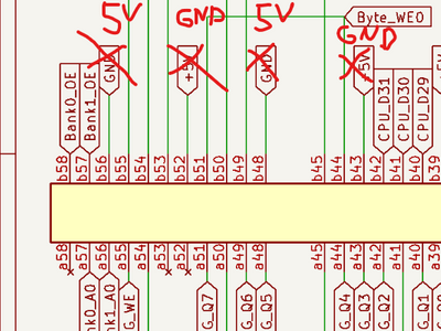
Smells like a short between 5v and ground, and PSU is shutting down. Suspicion is currently if we have the slot pin out correct, as the module did not have any unexpected shorts.
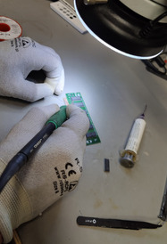
My friend who is helping with soldering work, will probably clarify.
Last edited by RockstarRunner on 2024-02-28, 20:14. Edited 1 time in total.
Just small clarification, I added wires to 5V and GND just using CT1 as soldering point and used oscilloscope to check what happens with powerline as computer didn't react at all and it looked like 5V started to come up and shut down immediately. My brain is currently lacking any blood circulation after hard training, so I might have missed something but module itself looks good now.
B56 - 30 Ohms to the ground this is 5V not GND like in schema
B52 - 0 Ohms to the ground, this is GND, not 5V like in schema
B48 - 30 Ohms to the ground this is 5V not GND like in schema
B43 - 0 Ohms to the ground, this is GND, not 5V like in schema
Puuh - happy I got it right in post "2024-02-05, 17:15".
This should be easy to fix in layout "Rev. 1.1".
Congrats to everyone!
Would have helped if I had looked back the thread when I realized that there was short between 5V and GND. And of course rockstarrunner sent me the link to that post after I said I found at least one mixed 5V/GND, but I was just measuring every effing pin just then and did not notice. Why do things easily if you can do them hard way, that is where all the fun is 😁
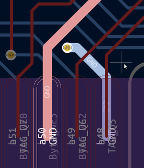
Ironically I think power and ground on the cache connector itself are the only things I wont be able to deduce from images, every 4th pin is a ground stich, but might be power.
thank you, will incorporate in final version.
You want to hear something funny? While routing b48 (blue) it looked very wrong to me 😀 Wrong to the point I started scratching my head and questioning original designer. b48 trace sharply turns left before stitching to the ground plane, and the via it uses is right next to a50 track (orange) which is also supposed to be ground. Why would anyone design it like that and not make a50 track touch the via, why not just turn right instead (where the cursor is)?
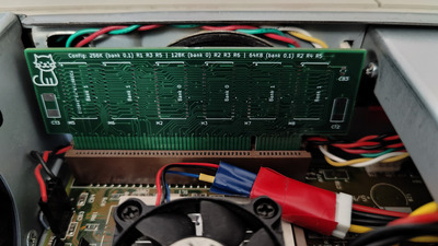
Time for some benchmarks, cachechk and doom (fastdoom is easier to benchmark). Im really curious about 128/64KB difference, and if 64KB setting works at all.
This is probably fine as it is but going to add some wires there.
yeah, I wouldnt bother with wires, this excessive power/ground stitching is for lowering impedance, wires will probably make it worse.
Could I please trouble you for few photos of assembled module, both sides lose and in its final resting place installed in motherboard inside the case?