First post, by mita
I am going to share my experiment building this project, see the following links. In short: how to use non 5V CPU like AMD 5x133 in a 486 5V ONLY MB.
https://github.com/scrapcomputing/486SocketBl … =readme-ov-file
https://www.youtube.com/watch?v=vEpAoVE4KjU
I drew the following build consequences:
- You have to know the main fact: one error in the preparation or in the soldering could result a failure, you have to start again. Order more PCB, DC-DC converter and pins to be able to start over.
- You have to be very carefull handling all the pins: the processor's pins should be in-line in both direction. A minuscule bent pin will block the insertion of the processor to the new socket. Add a small dimensional error on the female pins and you will realize it is no way to socket the cpu into the new socket.
-When you soldered a new row of pins try the cpu to fit or try the adapter to fit into the MB. At the beginning it will be easy but adding more and more rows the insertion will became more and more difficult. The purpose of this "mating" is to form the male pins to the female pins. In this way you have to deal with one line of a "problem" only. If mating is easy than the soldered row of pin is perpendicular to the PCB and the ends of the row is grinded well. This grinding is very important: a "sticking out" end of row will push the next row which can not be perpendicular to the PCB. If not perpendicular the mating will not be possible.
- Check every steps. You can not make any mistakes. One mistake will render the build useless. Check every end of the rows, grind back the ends. Solder the two endpoints of a row and check the perpendicularity of the row. If it is ok than solder the other pins. Check every soldered pins under magnification. I found many times the pin absorbed the tin but the pad is not. The size of the pad is small and it is easy to left it without tin. 12x magnification is recommended. Resolder every pin which is suspectible.
- Handle the solder with attention. It is very easy to fill other pads unintentionally. It is not easy to remove the tin from these pads-holes
- Check the continuity of the newly soldered top-bottom pins and the surrounding pins for short. If you made a bad soldering than this is the time to be able to correct it. if you solder the next paralell row than you do not have a canche to correct it. It is a garbage. Start over.
- The sequence of the solderig of the rows are very important. See the github documentation and the video. The white circles on the board designates the first pin of a given row, helping the placement process. Do not forget to altering the sides and solder the male - female rows alternate. This is the only way to solder every pin. Miss one alteration and it is done. Start over.
- Use a soldering tip suitable to this job. Too small will not be able to transfer the heat, too big will mess with the adjacent pins and pads. Use right temperature: do not melt the plastic but be able to quickly do the soldering. Clean the board before the soldering with IPA. Use flux if there is a difficulty to tint the pads around the pins. Clean the flux after the soldering with IPA (bath).
- Check the DC-DC converter before soldering in to the socket. Use an 2 ohm/10W resistor to simulate the load and measure the ripple with the scope. Check the thermal condition of the converter. Please note the converter will be in a much hotter place next to the bottom of the CPU. Use high efficiency converter (90% or more in case of 5V in, 3.5V out, 2A load). Trace down the converter IC and check the datasheet, do not accept blindly the seller's data. Use at least 0.8mm wires to solder the converter into its place. The thicker the better. If the MB suddenly stops working in the middle of a stressfull session than probably the thermal shutdown of the converter IC initiated. All your current work - progress will be lost. This is one reason why the cooling of the CPU is so much important. I think this is one of the weakest spot of this design but that is it.
-Check the ripple and the voltage when the system is under stress. The voltage range should be within 5%. The ripple should be less than 20mV.
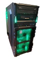
- Count on problems: sart with MB settings first with the jumpers to check the MB operation. If it is ok than use the multiplication jumper to go higher internal clock. The result can vary MB to MB. In case of a Hypo MB the 133MHz internal clock was too high to boot from IDE, the system hanged. In case of 100MHz it was ok. On Acer A1 board 133MHz clock was ok. Switching off the Acer A1 - but keep the STBYON - and switching on again resulted a stuck boot process. Reset cured it 98% of times. But if you switched off and removed the power cord it starts without any problem. Strange.
- I found this job a difficult one. It takes a lot of time and effort to work with full attention. A lot of possibility of errors. And of course a merit at the end. The system is definitely more speedy with an amd 5x133 comparing to the 486DX33. Does it worth it? The material cost is much higher than the price of the 5x133 not counting the assembly time. Mixed feeling. But hey. More ridicioulos upgrades are in the horizont regarding the Acer A1 MB. Good luck!