VOGONS


First post, by ontrca

User metadata
Rank Newbie
Rank
Newbie

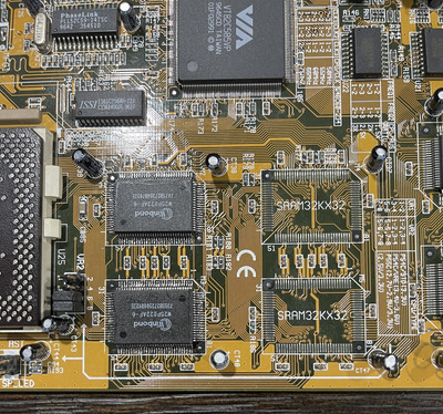
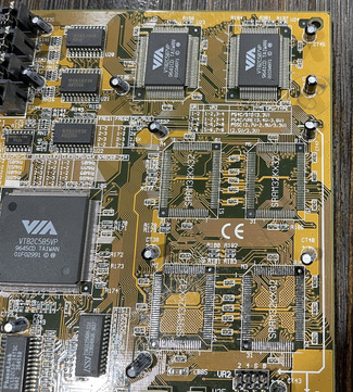
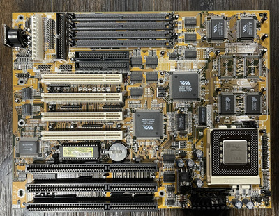
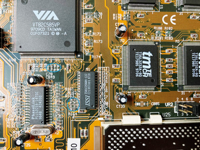
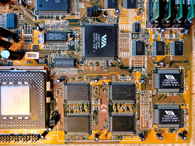
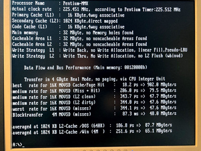
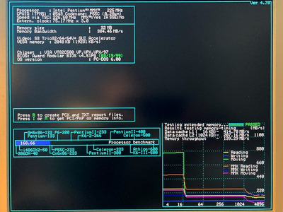
I have a FIC PA-2005(v1.3) motherboard with 256k cache factory soldered onboard.

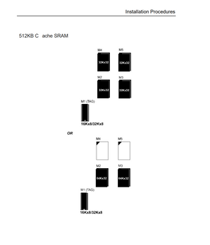
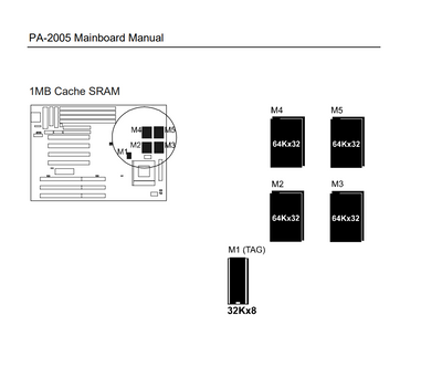
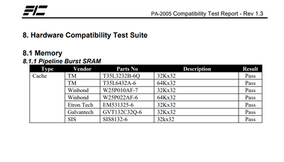
According to the manual it is upgradable to 512k or 1mb and compatible
with (Winbond W25P022AF-6 64Kx32) Pipeline Burst SRAM.

So that's what I bought.
I am doing the cache upgrade myself (or trying to) 😀

I desoldered the 2 old chips and soldered on 2 of the new chips for a total of 512k to test before I went through the trouble of soldering the whole 1mb (4 chips).
In case you're wondering I tested everything, and all the contacts are good, and nothing is shorted together 😀

But then I read online that you have to change some onboard resistors or something??

Also In order to upgrade to 512KB/1MB cache it needs a 32Kx8 TAG but it came with one from the factory so it's good to go 😀

So that is my question..., can anyone help me? Does anyone know what resistors or whatever I'm supposed to change? 😀

Attachments

  • IMG_9471.jpg
    Filename
    IMG_9471.jpg
    File size
    1.2 MiB
    Views
    360 views
    File license
    Public domain
  • IMG_9428.jpg
    Filename
    IMG_9428.jpg
    File size
    908.82 KiB
    Views
    360 views
    File license
    Public domain
  • IMG_9395.jpg
    Filename
    IMG_9395.jpg
    File size
    1.14 MiB
    Views
    360 views
    File license
    Public domain

Reply 1 of 14, by majestyk

User metadata
Rank Oldbie
Rank
Oldbie

I can tell you the jumpering for 512K, I upgraded two of my PA-2005 a while ago. I never bothered trying 1MB because I usually don´t need 256MB RAM on mainboards like this.

You should also populate Jumper "CLK3" and try if 75 MHz FSB runs stable. In most cases it does.

Reply 2 of 14, by douglar

User metadata
Rank Oldbie
Rank
Oldbie

Sounds like an exciting project. I don't see anything in the manual for selecting the cache size, but I guess that's not a surprise since it wasn't supposed to be user selectable.

Have you upgraded the BIOS?
https://theretroweb.com/motherboards/s/fic-pa-2005#bios

Reply 3 of 14, by ontrca

User metadata
Rank Newbie
Rank
Newbie
majestyk wrote on 2024-05-15, 05:36:

I can tell you the jumpering for 512K, I upgraded two of my PA-2005 a while ago. I never bothered trying 1MB because I usually don´t need 256MB RAM on mainboards like this.

You should also populate Jumper "CLK3" and try if 75 MHz FSB runs stable. In most cases it does.

I'd appreciate any type of help 😀 Thank You 😀

Reply 4 of 14, by ontrca

User metadata
Rank Newbie
Rank
Newbie
douglar wrote on 2024-05-15, 12:51:

Sounds like an exciting project. I don't see anything in the manual for selecting the cache size, but I guess that's not a surprise since it wasn't supposed to be user selectable.

Have you upgraded the BIOS?
https://theretroweb.com/motherboards/s/fic-pa-2005#bios

I was thinking about that but wasn't sure if it would help 😀
I'll try it 😀 Thank You 😀

Reply 5 of 14, by ontrca

User metadata
Rank Newbie
Rank
Newbie
ontrca wrote on 2024-05-19, 00:09:
douglar wrote on 2024-05-15, 12:51:

Sounds like an exciting project. I don't see anything in the manual for selecting the cache size, but I guess that's not a surprise since it wasn't supposed to be user selectable.

Have you upgraded the BIOS?
https://theretroweb.com/motherboards/s/fic-pa-2005#bios

I was thinking about that but wasn't sure if it would help 😀
I'll try it 😀 Thank You 😀

I updated to this BIOS from "theretroweb.com"
"07/15/97-VT82C580VP-2A5LA008C-00 Vobis OEM 4.51PG VBS1.03D8"
And that didn't help :3

Reply 6 of 14, by majestyk

User metadata
Rank Oldbie
Rank
Oldbie

For a 512K configuration you must move R162 (0 ohm) to position R161 for connecting A13 of the TAG chip to the chipset and R148 (0 ohm) to position R147 for connecting CA 18 = Pin34 of the C585VP to the cache chips.

pa_2005_512Ka.JPG
Filename
pa_2005_512Ka.JPG
File size
1.45 MiB
Views
196 views
File license
Fair use/fair dealing exception

For 1M cache you will also have to connect address line A14 of the TAG chip to the chipset by adding a 0 ohm resistor at position R164. After that the modifications at the TAG chip are complete.
You also will have to modify the resistors at the C585VP to connect address line CA19 = pin35 to the cache chips. You do this by adding a 0 ohm resistor at position R150.

Reply 9 of 14, by ontrca

User metadata
Rank Newbie
Rank
Newbie
majestyk wrote on 2024-05-19, 07:00:
For a 512K configuration you must move R162 (0 ohm) to position R161 for connecting A13 of the TAG chip to the chipset and R148 […]
Show full quote

For a 512K configuration you must move R162 (0 ohm) to position R161 for connecting A13 of the TAG chip to the chipset and R148 (0 ohm) to position R147 for connecting CA 18 = Pin34 of the C585VP to the cache chips.
pa_2005_512Ka.JPG

For 1M cache you will also have to connect address line A14 of the TAG chip to the chipset by adding a 0 ohm resistor at position R164. After that the modifications at the TAG chip are complete.
You also will have to modify the resistors at the C585VP to connect address line CA19 = pin35 to the cache chips. You do this by adding a 0 ohm resistor at position R150.

Well dang that sucks 🙁
My 512k cache upgrade still doesn't work.
I followed your 512K configuration and,
I checked all of my solder points again for shorts and stuff and everything seems to be correct but still not working 🙁

Maybe one of my cache chips are bad 🙁

Reply 10 of 14, by majestyk

User metadata
Rank Oldbie
Rank
Oldbie

I always used a 4-chip 32Kx32 setup for 512K so far. I never cared if and how the A15 pins of the chips are wired and weather they are connected to the chipset.
On the silkscreen printing the 4 positions are marked "32K x 32", but that doesn´t necessarily mean 64Kx32 chips are not supported - at least the A15 pins (pin 49) are connected in some way.
Maybe I will try 4 chips 64Kx32 next week

Reply 11 of 14, by ontrca

User metadata
Rank Newbie
Rank
Newbie
majestyk wrote on 2024-05-20, 07:16:

I always used a 4-chip 32Kx32 setup for 512K so far. I never cared if and how the A15 pins of the chips are wired and weather they are connected to the chipset.
On the silkscreen printing the 4 positions are marked "32K x 32", but that doesn´t necessarily mean 64Kx32 chips are not supported - at least the A15 pins (pin 49) are connected in some way.
Maybe I will try 4 chips 64Kx32 next week

According to the manual the motherboard supports 64Kx32 chips in 512k and 1mb configurations 😀

Attachments

Reply 12 of 14, by ontrca

User metadata
Rank Newbie
Rank
Newbie
majestyk wrote on 2024-05-20, 07:16:

I always used a 4-chip 32Kx32 setup for 512K so far. I never cared if and how the A15 pins of the chips are wired and weather they are connected to the chipset.
On the silkscreen printing the 4 positions are marked "32K x 32", but that doesn´t necessarily mean 64Kx32 chips are not supported - at least the A15 pins (pin 49) are connected in some way.
Maybe I will try 4 chips 64Kx32 next week

And also according to the manual the motherboard is compatible with the cache chips that I bought 😀

Attachments

Reply 13 of 14, by majestyk

User metadata
Rank Oldbie
Rank
Oldbie

Today I put 4 64K x32 chips on one of my PA2005 and it´s working perfectly.

There´s one thing I forgot to mention:
When you add the 0 Ohm resistor at position R150 you must also remove the one at position R147 (and R148 if present).

pa20051ma.JPG
Filename
pa20051ma.JPG
File size
1.74 MiB
Views
28 views
File license
Public domain
ctcm1m.JPG
Filename
ctcm1m.JPG
File size
239.68 KiB
Views
47 views
File license
Public domain
spsys1m.JPG
Filename
spsys1m.JPG
File size
205.5 KiB
Views
47 views
File license
Public domain

L2 is just 25% faster than RAM. If there are some hidden settings for timings in this BIOS it might be worth playing with them.

Last edited by majestyk on 2024-05-22, 18:25. Edited 3 times in total.