VOGONS


PGA132 rotator boards

Topic actions

Reply 60 of 116, by Sphere478

User metadata
Rank l33t++
Rank
l33t++

Okay, adding extra layers for ground didn’t go well. I need 11 or 13 layers and options are 10 and 12.

So… 6 it is! I guess we see how bad it really needs a ground layer with a prototype? (Later)

This probably has some errors still, let’s call it a potentially functional beta. But a more refined one will soon follow. Don’t order this.

Attachments

  • 3d.png
    Filename
    3d.png
    File size
    210.09 KiB
    Views
    1161 views
    File license
    Public domain
  • blue.png
    Filename
    blue.png
    File size
    148.6 KiB
    Views
    1161 views
    File license
    Public domain
  • Filename
    386 rotator beta 3.14.zip
    File size
    309.95 KiB
    Downloads
    42 downloads
    File license
    Public domain
Last edited by Sphere478 on 2022-12-29, 07:19. Edited 1 time in total.

Sphere's PCB projects.
-
Sphere’s socket 5/7 cpu collection.
-
SUCCESSFUL K6-2+ to K6-3+ Full Cache Enable Mod
-
Tyan S1564S to S1564D single to dual processor conversion (also s1563 and s1562)

Reply 61 of 116, by Sphere478

User metadata
Rank l33t++
Rank
l33t++

layers

Attachments

  • pink.png
    Filename
    pink.png
    File size
    63.06 KiB
    Views
    1161 views
    File license
    Public domain
  • orange.png
    Filename
    orange.png
    File size
    52.57 KiB
    Views
    1161 views
    File license
    Public domain
  • green.png
    Filename
    green.png
    File size
    60.72 KiB
    Views
    1161 views
    File license
    Public domain
  • teal.png
    Filename
    teal.png
    File size
    54.81 KiB
    Views
    1161 views
    File license
    Public domain
  • red.png
    Filename
    red.png
    File size
    145.03 KiB
    Views
    1161 views
    File license
    Public domain

Sphere's PCB projects.
-
Sphere’s socket 5/7 cpu collection.
-
SUCCESSFUL K6-2+ to K6-3+ Full Cache Enable Mod
-
Tyan S1564S to S1564D single to dual processor conversion (also s1563 and s1562)

Reply 62 of 116, by Sphere478

User metadata
Rank l33t++
Rank
l33t++

The final version (and the latest one I haven’t uploaded) will be covered in silk btw to make bga less risky/easier.

The 270* one will just be a flipped/inverted version of this. The 180 will be two stacked bga style.

Feiopa, do you know what pins/sockets you will use?

Any thoughts as to assembly?

Sphere's PCB projects.
-
Sphere’s socket 5/7 cpu collection.
-
SUCCESSFUL K6-2+ to K6-3+ Full Cache Enable Mod
-
Tyan S1564S to S1564D single to dual processor conversion (also s1563 and s1562)

Reply 63 of 116, by feipoa

User metadata
Rank l33t++
Rank
l33t++

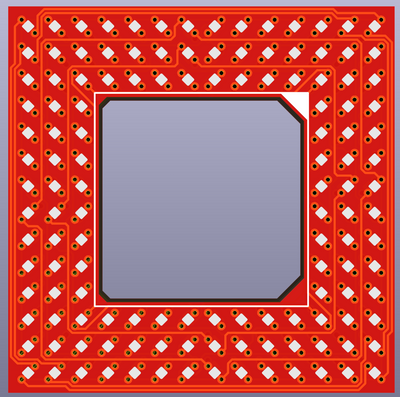
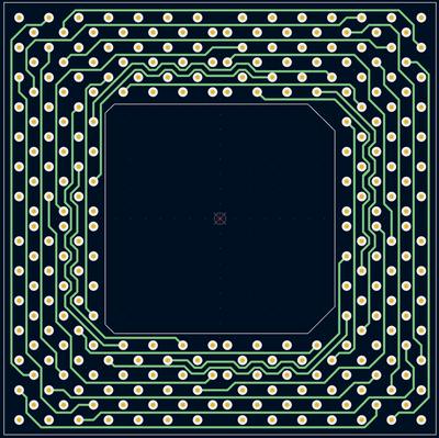
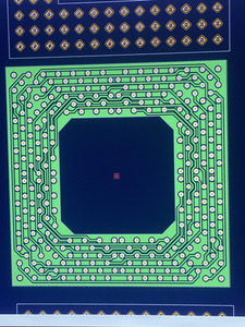
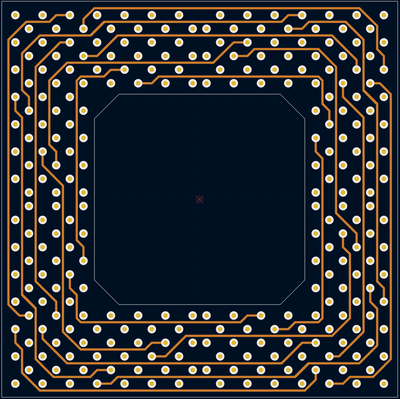
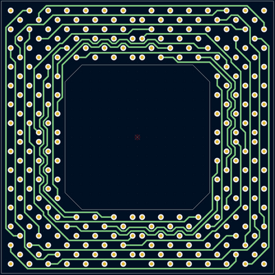
Looking at costing options, I noticed that for the SXL2 interposer, the following:

6-layer is $60, sale is $2
8-layer is $86, sale is $2
10-layer is $187
12-layer is $257

The cost to prototype 6-layer is $26 more than 8-layer. So if I needed to run a beta 1 and then beta 2 batch, the cost would be $120. if we do 8-layer and add ground plates between the data/address planes, it is $86. Seems like 8-layer is the way to go, assuming the first prototype works well.

10- and 12- layer are far too cost prohibitive.

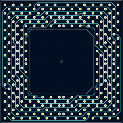
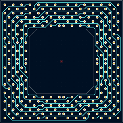
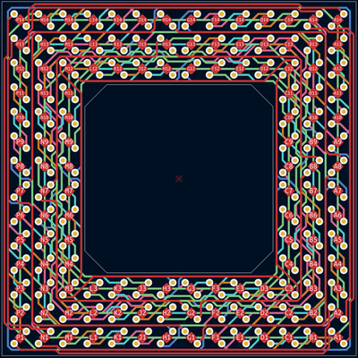
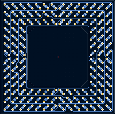
Why don't you want traces going through the middle? Seems like the middle region would be the preferred approach because traces would be going past less signals/traces. Also, less probability of having an issue with solder shorting the trace to PGA pin pads. Whatever the case, you'd still want to have physical PCB material in the middle for rigidity.

Regarding assembly, what is the difference between SMD and BGA for this application? I don't think I can BGA solder a 2-piece PCB sandwich together with any degree of certainty. The probability for a bridge is too high, and it won't be visible. Any mistake and the unit would need to be disassembled.

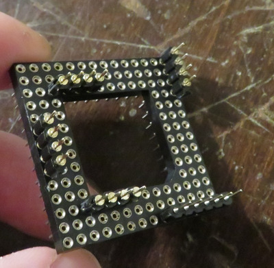
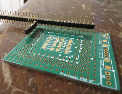
My idea was to have a single PCB with both sides as surface mount for the PGA pins.

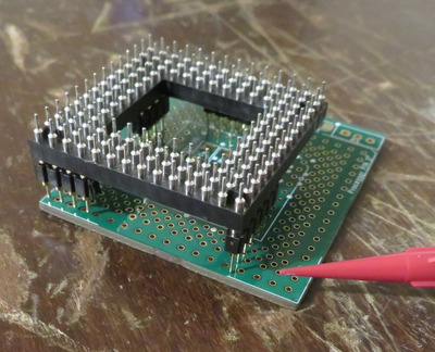
Then I would take the same male-to-male PGA pins used with the SXL2 interposer and place them into a temporary PGA132 (386) socket. The purpose of this socket is for alignment only. In the photo, I'm only showing a few rows of pins, but during assembly, 132 pins would be inserted.

1-put_male-male_pins_in_386_socket_for_alignment.JPG
Filename
1-put_male-male_pins_in_386_socket_for_alignment.JPG
File size
228.07 KiB
Views
1128 views
File license
CC-BY-4.0

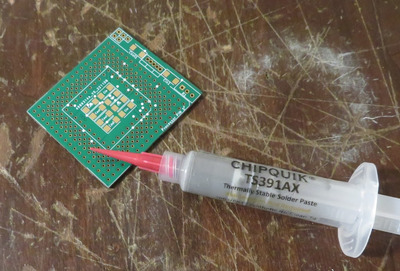
Next, apply solder paste to one of the sides of the PCB.

2-add_solder_paste_onto_bare_PCB_with_SMD_pads.JPG
Filename
2-add_solder_paste_onto_bare_PCB_with_SMD_pads.JPG
File size
185.26 KiB
Views
1128 views
File license
CC-BY-4.0

Now place the male-to-male PGA pins with the 386 socket attached onto the solder paste.

3-add_set_pins_and_socket_over_solder_paste.JPG
Filename
3-add_set_pins_and_socket_over_solder_paste.JPG
File size
194.45 KiB
Views
1128 views
File license
CC-BY-4.0

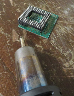
Use hot air to solder these PGA pins in place.

4-use_hot_air_to_solidify_the_solder_paste.JPG
Filename
4-use_hot_air_to_solidify_the_solder_paste.JPG
File size
116.24 KiB
Views
1128 views
File license
CC-BY-4.0

Then remove the 386 socket. Proceed to the other side of the PCB, but instead of using male-to-male PGA pins, we'd use male-to-female pins.

5-remove_the_386_socket_and_left_with_the_result.JPG
Filename
5-remove_the_386_socket_and_left_with_the_result.JPG
File size
182.62 KiB
Views
1128 views
File license
CC-BY-4.0

I would need to use a fairly generous amount of solder paste to ensure the PGA pins are held tight enough to the PCB. Ideally PGA pins with shorter legs would be preferred.

Plan your life wisely, you'll be dead before you know it.

Reply 64 of 116, by Sphere478

User metadata
Rank l33t++
Rank
l33t++

The routing is ring shaped, the problem is ring shaped, routing through the middle isn’t really a solution so much as it would just get in the way and make it harder to route. (And messier) I didn’t avoid it, it’s just how the traces wanted to route in the shortest most even way possible.

Doing it with separate strip sockets is going to be a problem. These pads might lift. You want a full socket if you can manage it. On the bottom actual processor pins might be acceptable held in place with a zif or lif while soldering. Or some kinda jig.

I don’t think bga stacking this will be as hard as you think. Encourage you to look into the tools required.

I can make you a paste mask you can order out of 0.6 pcb possibly. Or talk with jlc about one maybe out of metal.

Sphere's PCB projects.
-
Sphere’s socket 5/7 cpu collection.
-
SUCCESSFUL K6-2+ to K6-3+ Full Cache Enable Mod
-
Tyan S1564S to S1564D single to dual processor conversion (also s1563 and s1562)

Reply 65 of 116, by feipoa

User metadata
Rank l33t++
Rank
l33t++

Since not doing through hole, the approach I have presented is the only viable approach for me to assemble the unit. Of course, for $2, I can try BGA two sandwitch layers, but I don't think this is a good approach for the masses. Is it not possible to make this as a single PCB in 8-layer?

Regardless of BGA or no BGA, there is no simple solution for adhering machine pins. I could not locate a single PGA132 male-male or male-SMD machine pin array. When I looked at how other companies have done this, it appears that they are using partially submerged vias. I think you called this "blink via". Last I spoke with JLCPCB, they do not offer this.

With my approach, those PGA row pins would be epoxied between them to increase rigidity throughout the whole array. I won't be easy to lift just one pad - you'd have to take at least a half dozen at the same time, which is not likely. The interposer would come out of the motherboard before the pads were lifted. If using a proper PGA CPU removal tool, I don't think lifting pads will be an issue.

Plan your life wisely, you'll be dead before you know it.

Reply 66 of 116, by Sphere478

User metadata
Rank l33t++
Rank
l33t++

Epoxy or super glue, or something. That might help. 🤔 good idea.

Idk about 8 layer 180 unless I try but conventional wisdom says 12 layers.

I can do more of the squiggly stuff to increase density but it only gets me so far.

This is many hours of work btw.

Btw, I don’t see why you couldn’t bga a flat pga pcb to both sides of this. To make a blind via setup.

Sphere's PCB projects.
-
Sphere’s socket 5/7 cpu collection.
-
SUCCESSFUL K6-2+ to K6-3+ Full Cache Enable Mod
-
Tyan S1564S to S1564D single to dual processor conversion (also s1563 and s1562)

Reply 67 of 116, by Sphere478

User metadata
Rank l33t++
Rank
l33t++

In fact, let that be the new plan.

Pga blank thru hole pcb with holes and pads but no traces

Rotator

Second rotator

Pga blank thru hole pcb with holes and pads but no traces

Bga them all together.

Thoughts?

It may be possible to mechanically connect some of the pcbs so that connection happens when soldering the pins one by one after bga in the middle on 180 or no bga on the stack of three (blank roator blank)

Sphere's PCB projects.
-
Sphere’s socket 5/7 cpu collection.
-
SUCCESSFUL K6-2+ to K6-3+ Full Cache Enable Mod
-
Tyan S1564S to S1564D single to dual processor conversion (also s1563 and s1562)

Reply 68 of 116, by Sphere478

User metadata
Rank l33t++
Rank
l33t++
image.jpg
Filename
image.jpg
File size
1.57 MiB
Views
1083 views
File license
Public domain

Btw, here is the hopeless situation with copper flood. And why I haven’t poured copper between the tracks. Nothing will connect.

I did another pass over the traces and pcb and corrected a number of errors. At this point I will post another screen of the layers and ask for Feiopa to double check to make sure it looks okay. I’ll continue to check it and probably find some more stuff. But it’s winding down on the 90 degree board. Should be ready for a prototype soon.

Once this is settled I will do a few 180 degree experiments.

I’m sure it can be done, the question is how many layers.

I think more than 8.

And the other question is, which is better, two sacked 90s or one 180. I think the stacked 90s might have better EMI properties. Thoughts?

I also need to make a mirror image of this one for the 270 but I’ll do that after this one is debugged.

Sphere's PCB projects.
-
Sphere’s socket 5/7 cpu collection.
-
SUCCESSFUL K6-2+ to K6-3+ Full Cache Enable Mod
-
Tyan S1564S to S1564D single to dual processor conversion (also s1563 and s1562)

Reply 69 of 116, by Sphere478

User metadata
Rank l33t++
Rank
l33t++

layers and 3d

Attachments

  • teal.png
    Filename
    teal.png
    File size
    105.53 KiB
    Views
    1074 views
    File license
    Public domain
  • red.png
    Filename
    red.png
    File size
    257.01 KiB
    Views
    1074 views
    File license
    Public domain
  • pink.png
    Filename
    pink.png
    File size
    114.98 KiB
    Views
    1074 views
    File license
    Public domain
  • PGA To BGA Shim.png
    Filename
    PGA To BGA Shim.png
    File size
    81.64 KiB
    Views
    1074 views
    File license
    Public domain
  • 3d.png
    Filename
    3d.png
    File size
    89.28 KiB
    Views
    1074 views
    File license
    Public domain

Sphere's PCB projects.
-
Sphere’s socket 5/7 cpu collection.
-
SUCCESSFUL K6-2+ to K6-3+ Full Cache Enable Mod
-
Tyan S1564S to S1564D single to dual processor conversion (also s1563 and s1562)

Reply 70 of 116, by Sphere478

User metadata
Rank l33t++
Rank
l33t++

edit: old files don't use
layers and files

Attachments

  • Filename
    386 rotator Beta 3.1415.zip
    File size
    1.72 MiB
    Downloads
    43 downloads
    File license
    Public domain
  • all layers.png
    Filename
    all layers.png
    File size
    381.32 KiB
    Views
    1071 views
    File license
    Public domain
  • blue.png
    Filename
    blue.png
    File size
    262.04 KiB
    Views
    1071 views
    File license
    Public domain
  • orange.png
    Filename
    orange.png
    File size
    99.18 KiB
    Views
    1071 views
    File license
    Public domain
  • green.png
    Filename
    green.png
    File size
    112.91 KiB
    Views
    1071 views
    File license
    Public domain
Last edited by Sphere478 on 2023-01-04, 07:28. Edited 3 times in total.

Sphere's PCB projects.
-
Sphere’s socket 5/7 cpu collection.
-
SUCCESSFUL K6-2+ to K6-3+ Full Cache Enable Mod
-
Tyan S1564S to S1564D single to dual processor conversion (also s1563 and s1562)

Reply 71 of 116, by Sphere478

User metadata
Rank l33t++
Rank
l33t++

Of course as you know, you can ignore the silk covering the pads on 3d that disappears when I generate the gerbers.

Sphere's PCB projects.
-
Sphere’s socket 5/7 cpu collection.
-
SUCCESSFUL K6-2+ to K6-3+ Full Cache Enable Mod
-
Tyan S1564S to S1564D single to dual processor conversion (also s1563 and s1562)

Reply 72 of 116, by feipoa

User metadata
Rank l33t++
Rank
l33t++

I could try to BGA a flat PCB to the upper and lower layers of the core PCB to mimic blind vias, but with increased complexity comes increased probability of goofing up during assembly. Are you suggesting this just to increase the strength of the PGA pins onto the PCB? I don't think the PGA to surface mount idea is all that bad once the PGA pins are JB welded together. You could also create a standard PGA-132 PCB for me to solder the male-to-male pins though, then surface mount this to the core PCB.

If I understand you correctly, these pseudo blind via PCB's will have 132 through-hole pins on both sides, but on the inner layer you'd cover the via with silk screen. The bottom of the pseudo-board would have another 132 pads set between the standard PGA-132 pin spacing (as you've shown). I would then, either have the offset 132 BGA pins pre-balled, or not balled at all, but have solder paste put on them. I'd then hot air this layer onto the core PCB. Once it is hot aired onto the core to make a sandwich, I would solder the PGA pins on using an iron through the outer layer. Then repeat for the other side.

I can try it for $2 each PCB, but I think the distance from those diamond shaped pads to adjacent pads is too close. Without it being factory placed and soldered, I see a 99.9% chance of a short occurring, either because of solder overflow, or due to a hair off in alignment. I think you'd want to entirely eliminate those diamond shaped BGA pads on the core PCB's top/bottom layer. The upper and lower sandwich layers can either be offset by 1.8 mm during assembly, or, can be placed on square if the pseudo boards loose the 'between PGA solder pads'.

In doing so, the core PCB should still be usable with my original plan and your sandwich method. I would most likely start with my orignal plan, ensure the rotator board works, then start experimenting with this BGA sandwitch to increase pin strength (if needed).

In my reply thus far, I am assuming the item you have identified as "PGA to BGA Shim" is the same PCB as "PGA132 Rotator", just one is the top layer, the other is the bottom layer of the same PCB. If this is not the case, then I don't follow what you've presented.

Plan your life wisely, you'll be dead before you know it.

Reply 73 of 116, by Sphere478

User metadata
Rank l33t++
Rank
l33t++

I’m not following your reply.

There are now two pcbs project files in the zip

One is just a pga socket pad array

And the other is the rotator.

Alignment won’t be an issue it’s 2.54mm between pads everything we don’t want to stick is covered with silk.

The pga socket array pcb you clamp down to the rotator on both sides. Maybe you fill it with solder paste and push the socket in idk.

Or solder it then melt the rotator to it with hot air. Idk, you’ll have to try it out if it doesn’t work, j and b weld.

Let me know.

Look over the last screenshots and tell me if anything looks wrong and I’ll fix it. Here in the next few days I’ll take another look also. But should be ready for prototype soon

Last edited by Sphere478 on 2023-01-01, 00:09. Edited 1 time in total.

Sphere's PCB projects.
-
Sphere’s socket 5/7 cpu collection.
-
SUCCESSFUL K6-2+ to K6-3+ Full Cache Enable Mod
-
Tyan S1564S to S1564D single to dual processor conversion (also s1563 and s1562)

Reply 74 of 116, by feipoa

User metadata
Rank l33t++
Rank
l33t++

I was asking if you can produce a variant without those diamond shaped pads between the 132 pins, but rather make the solder pads be at the location of the 132 pins.

Plan your life wisely, you'll be dead before you know it.

Reply 75 of 116, by Sphere478

User metadata
Rank l33t++
Rank
l33t++

Those diamond shaped pads are at the location of the pga 132 pins

Btw, here is an example of how the silk is clearanced after gerber generation.

This showed as pads covered on 3d view prior to mfg.

file.php?id=152678&mode=view

Attachments

Sphere's PCB projects.
-
Sphere’s socket 5/7 cpu collection.
-
SUCCESSFUL K6-2+ to K6-3+ Full Cache Enable Mod
-
Tyan S1564S to S1564D single to dual processor conversion (also s1563 and s1562)

Reply 76 of 116, by feipoa

User metadata
Rank l33t++
Rank
l33t++

Are you willing to provide a variant which only has straight through PGA-132 pins on the "shim", no pads in-between on the other side. Would you also be able produce a core PCB which does not use those diamond pads between the PGA pins, and only has these diamond SMD pads where the existing vias are (and no silkscreen over the vias)?

For $2, I am willing to try your idea, but for another $2, I'd like to have another option (my plan). Or, if you are planning on doing the assembly, please nevermind my request.

Plan your life wisely, you'll be dead before you know it.

Reply 77 of 116, by Sphere478

User metadata
Rank l33t++
Rank
l33t++
feipoa wrote on 2023-01-01, 04:24:

Are you willing to provide a variant which only has straight through PGA-132 pins on the "shim", no pads in-between on the other side. Would you also be able produce a core PCB which does not use those diamond pads between the PGA pins, and only has these diamond SMD pads where the existing vias are (and no silkscreen over the vias)?

For $2, I am willing to try your idea, but for another $2, I'd like to have another option (my plan). Or, if you are planning on doing the assembly, please nevermind my request.

Feiopa, I am having trouble understanding you. It sounds like you are describing what I already made. And some stuff that doesn’t make sense to me.

Can you draw a pic so we can get on the same page might be something lost in translation here 😀 I’m trying to understand you.

Sphere's PCB projects.
-
Sphere’s socket 5/7 cpu collection.
-
SUCCESSFUL K6-2+ to K6-3+ Full Cache Enable Mod
-
Tyan S1564S to S1564D single to dual processor conversion (also s1563 and s1562)

Reply 78 of 116, by Sphere478

User metadata
Rank l33t++
Rank
l33t++

But going off what you said, if you want pads over the vias on the rotator and no pads between the vias on the rotator then you wouldn’t be able to use it? The pads would be in the wrong place?

As for no pads/plated holes on the shim but only naked drill holes. That’s easy enough if that’s what you want. So is removing the silk from the rotator. I can whip that up in a few seconds. Can you help me understand your reasoning in wanting it that way, I’m curious.🤔 do you not want the solder to stick to the shim is that it? Why wouldn’t you want silk over the vias on the rotator? You were worried about solder sticking to them on the sxl2 interposer.

Sphere's PCB projects.
-
Sphere’s socket 5/7 cpu collection.
-
SUCCESSFUL K6-2+ to K6-3+ Full Cache Enable Mod
-
Tyan S1564S to S1564D single to dual processor conversion (also s1563 and s1562)

Reply 79 of 116, by Ozzuneoj

User metadata
Rank l33t
Rank
l33t

This may sound dumb, but would it be any benefit to have a design that made use of a couple different methods? For example, have the simplest (cheapest) PCB possible to cover as many pins as possible while using wire to relocate some pins that would require a far more complex PCB? Maybe even have ribbon cables twisted in the center to cover a couple rows? I know the idea of using twisted wire packed in epoxy\resin was suggestion earlier, but perhaps it is feasible if it this method isn't needed for every single pin. If it's a matter of looks, it could even be possible to encase the whole thing in a simple 3D printed frame or cartridge of sorts. You could route wires around the outside of the PCB that would otherwise not be possible without multiple layers, but it wouldn't be visible (ugly) if it were enclosed.

I have no experience with this stuff, I have just been intrigued by the "puzzle" you guys are working on and I can't shake that feeling that there must be some outside the box way to balance the cost of a complex PCB with ease of assembly.

Obviously a PCB (or multple PCBs) is the most elegant looking solution... but when getting into $60-$250 for these multi-layered boards, it's getting pretty pricey.

Again, you guys are obviously way more experienced at this than I could ever be, I just figured I'd toss some more ideas out there. 😀

Now for some blitting from the back buffer.